Back-Biased Packaging Advances (SE, SG, SH, and SJ versus SA and SB)
By Daniel Dwyer, Allegro MicroSystems, LLC
Abstract
In addition to advancements made in Hall sensor IC technology over the last decade, Allegro™ MicroSystems has also produced significant packaging advancements in back-biased devices. Magnetic circuit elements and the use of high temperature materials have resulted in lower total system costs for manufacturers using them in final sensor module products. Innovative package design and assembly technology have produced smaller, more powerful devices.
SA and SB Packaging
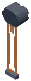
Allegro's SA and SB represent the first generation of back-biased packages. The SA and SB are composed of mechanically assembled components that are ultrasonically welded into a finished package. The molded Hall-effect IC provides the brain of the system, the pole piece and rare-earth pellet enhance the magnetic circuit, while the housing and end cap provide the package shell.
The SA and SB differ only in their size; the SB is 7 mm long while the SA is 9 mm long. The larger sized SA is used predominately for single-element Hall effect devices that require a larger, more complex magnet system than a differential device.
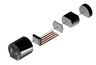
Figure 1. Exploded View of SA Differential Package.
SE, SG, SH, and SJ Packages
Like the SA and SB, the newer SE, SG, SH, and SJ packages possess all of the required elements for a gear tooth sensing IC. Unlike the SA and SB, the functional components of the new packages are assembled and then molded in a single step. Refer to figure 2 to see the cross section of the SB package and figure 3 to see the cross section of the SG package. The SG package cross section is also representative of the SE, SH, and SJ. The SE accomodates the larger, specially designed rare-earth pellet for TPO (True Power On) and proximity sensing, while the smaller SG, SH and SJ packages accept the differential pellets used for speed and direction sensing.
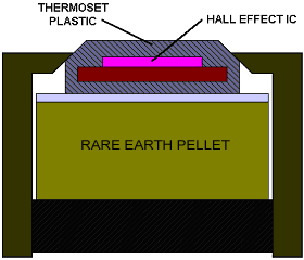
Figure 2. SB Package Cross-Section.
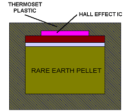
Figure 3. SG Package Cross-Section.
SE, SG, SH, and SJ Leadframes
These four packages have identical fabrication processes and package dimensions, they do possess distinctly different leadframes. The SE, SG, and SJ have four leads and are used with open-collector, 3-wire devices, while the SH has two wide leads for use with 2-wire devices. The two leads of the SH are wider than those of the SG to facilitate soldering or welding. The SE and SJ have narrower leads than the SH, but they are spread to facilitate soldering and welding.
 |
 |
 |
 |
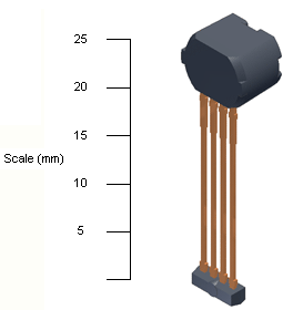
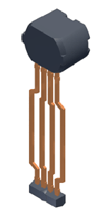
| SG | SH | SJ | SE |
|
Figure 4. Isometric Views of Advanced Packages. |
|||
In all four packages, the leads have been sized and spaced such that forming them against the package does not increase the outer diameter of the package case envelope.
A thermoplastic lead bar molded onto the end of the leads controls lead coplanarity and straightness during shipping and subsequent processing.
Molded features on the back of the packages facilitate orientation and location during subsequent assembly steps. Refer to figure 5.
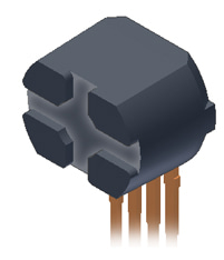
Figure 5. SG Package Isometric Showing Features on Reverse Side.
SE, SG, SH, and SJ Package Advantages
The patented Allegro SE, SG, SH, and SJ packages allow the rare-earth pellet to sit closer to the IC than it does in the first generation packaging (refer to figures 2 and 3). This geometric advantage allows the device to meet large air gap performance with a smaller pellet than that found in standard packages. The resultant small packages fit in the tight spacing dictated by today's gear-tooth sensing applications.
The clearances required for assembly in the SA and SB result in voids throughout the interior of the package (refer to figure 1). Since the SE, SG, SH, and SJ have no such voids, heat dissipation is improved and air entrapment that could occur during subsequent potting operations is eliminated.
A further improvement in heat dissipation is realized through the reduced heat conduction path present in the SE, SG, SH, and SJ packages. Because of the single step molding process, the layer of plastic normally seen between the IC's leadframe and the pellet is eliminated. The increased thermal conductivity signifies greater heat-sinking capacity by the pellet, allowing for operation at higher ambient temperatures. Refer to figure 3.
SE, SG, SH, and SJ Solution Advantages
- Small Package Size
Single step thermoset molding allows close pellet/IC proximity for increased magnetic efficiency and reduced pellet size. Single step thermoset molding step also allows for thinner walls and results in smaller package size. - Simple System Implementation
Back-biased package with optimized pellet in a small, robust package requires minimal expertise in magnetic circuit design. - High Temperature Operation
Single step thermoset molding for improved heat dissipation provides operation at elevated temperatures. - Robust Post-Processing
Single step molding eliminates voids and precludes the generation of air bubbles during potting or overmolding. - Easy Lead Soldering and Welding
The optimized lead configurations of the SE, SH, and SJ packages provide for simple soldering and welding.
|
Package Matrix Table |
||||||||
|---|---|---|---|---|---|---|---|---|
|
Package |
Fabrication |
Hall IC Type |
Interface |
Case Diameter |
Case Depth |
|||
|
Mechanical |
Molded |
Single |
Differential |
3-Wire |
2-Wire |
|||
|
SA |
X |
|
X |
X |
X |
|
9 |
9 |
|
SB |
X |
|
X |
X |
X |
X |
9 |
7 |
|
SE |
|
X |
X |
|
X |
|
10 |
7 |
|
SG |
|
X |
|
X |
X |
|
8 |
5.5 |
|
SH |
|
X |
|
X |
|
X |
8 |
5.5 |
|
SJ |
|
X |
|
X |
X |
|
8 |
5.5 |