Have Questions? Let us help!
We're passionate about innovation. Reach out and you'll hear back from an expert shortly.
One of our solution experts will be in touch with you shortly. Keep reading to learn more about our industry leading solutions.
Have questions about our industry-leading current sensor ICs? Look no further!
Check out our most frequently asked questions and answers. 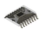
Parts can be ratiometric or non-ratiometric. Ratiometric indicates that the device sensitivity is proportional to the device supply voltage, VCC. In addition, the device output at 0 A, also called VIOUT(Q), is nominally equal to vcc / 2. Non-ratiometric devices will have VIOUT(Q) and sensitivity values stable over VCC variations within the specified input voltage range. Ratiometry can be useful when the input voltage of the sensor is on the same line as the ADC reference voltage. Non-ratiometric parts are useful in applications where the sensor input voltage is noisy or unstable. Unstable VCC will produce a noisy output if the part is ratiometric.
The three main types of error in current sensors are defined as:
Sensitivity Error: ESENS = (((Measured Sensitivity) / Sens) -1) × 100(%)
Offset Error: VOE = Measured QVO – QVO
Total Output Error: ETOT = ((VOUT – VOUT IDEAL )) / (Sensideal× IP ))× 100(%)
This application note goes more in depth on sources and definitions of error.
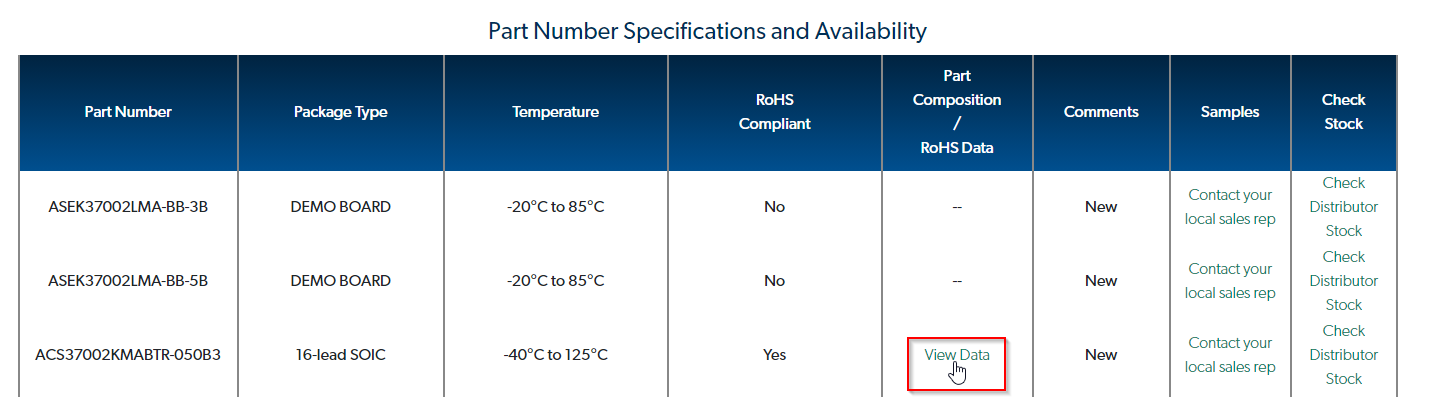
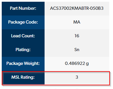
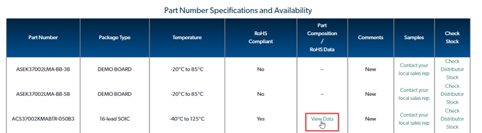
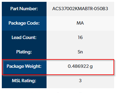
On the Allegro Current Sensor device homepage, navigate to the “Part Number Specifications and Availability”. Select “View Data” on the desired gain option. The MSL rating is included in the “Materials Declaration Report”.
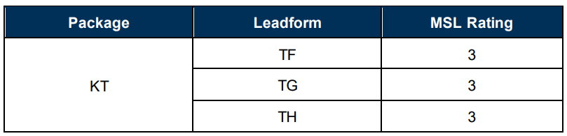
While MSL rating are specifically for surface mount parts, Allegro does qualify and provide a through hole equivalent (THD) for non-surface mount parts that directly correlates to the standard MSL ratings.
One of the key benefits of Hall Effect current sensors is their inherent galvanic isolation. Because there is no electrical connection between the primary current path and the signal circuitry, much higher working voltages are available. There are several isolation parameters or tests included in the current sensor device datasheets such as:
Dielectric Surge Strength- The amount of voltage that can be handled of a pulse of known rise time, width, and amplitude.
Dielectric Strength- The amount of voltage and time that can be withstood before electrical breakdown occurs. This is tested for a set amount of time (usually 60 seconds) while measuring leakage current to ensure breakdown has not occurred.
Working Voltage- The maximum voltage that can be continuously applied to the device. It usually has a specified value for DC, peak-to-peak, and RMS voltages.
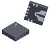
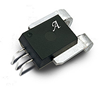
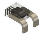
Isolation characteristics are specific to the package of the device. Below is a table summarizing the various packaging types offered by Allegro and their isolation characteristics as well as other important package information.
|
Package Descriptor |
SOICW-16 LA |
SOICW-16 MA |
SOICW-16 MC |
SOIC-8 LC1 |
SOIC-8 LC2 |
QFN-12 EXB |
7-pin PSOF LR |
5-pin CB |
|
Picture |
 |
 |
 |
 |
|
|
 |
|
|
Dimension |
10.3x10.3mm |
10.3x10.3mm |
11.3x13mm |
4.9x6mm |
4.9x6mm |
3x3mm |
6.4x6.4mm |
14x22mm |
|
Conductor Resistance |
0.85 mΩ |
0.85 mΩ |
0.27 mΩ |
1.2 mΩ |
0.65 mΩ |
0.6 mΩ |
0.2 mΩ |
0.1 mΩ |
|
Dielectric Strength |
RMS3600 V |
RMS5000 V |
RMS5000 V |
RMS2400 V |
RMS2400 V |
NA |
NA |
RMS4800 V |
|
Working Voltage |
DC870 V RMS616 V |
DC1550V RMS1097 V |
DC1618 V RMS1144 V |
DC420 V RMS297 V |
DC420 V RMS297 V |
DC100 V RMS70 V |
DC100 V RMS70 V |
DC1358 V RMS700 V |
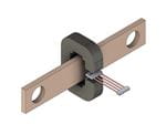
Allegro also offers core and coreless field sensors. These devices can sense currents >1000A and achieve >5000VRMS of dielectric strength isolation.
The part output will continue to increase or decrease until it reaches a high (current > IPR) or low (current < IPR) saturation point, where IPR is the current sensing range of the part. Voltage Output High/Low (VOH/VOL), sometimes referred to as Output Saturation Voltage (VSAT(H/L)), is defined as the voltage that sensor output, VIOUT, does not pass as a result to an increasing/decreasing magnitude of current. This can be seen in the figure below. Note that changing the sensitivity does not change the saturation voltage.
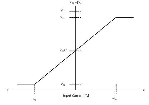
The functional range for the linear performance of VIOUT, and its related datasheet parameters, is valid from -IPR to +IPR. It is possible for the output to report voltages beyond the full-scale measurement until the saturation point, but parameters are not guaranteed beyond the full scale measurement.
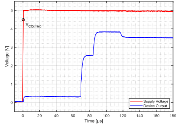
Every Allegro current sensor will have a power on time specified in the datasheet such as the example below:

Power-On Time, tPO , is defined as the time interval between a) the power supply has reached its minimum specified operating voltage (VCC(min)), and b) when the sensor output has settled within ±10% of its steady-state value under an applied magnetic field. An example of the output and supply voltage can be seen in the scope capture below:
Every Allegro current sensor includes pins for VCC, Ground (GND), VOUT, and a path for the primary current being sensed, if it is an integrated sensor. Some parts include additional pins for enhanced features. A list of these pins includes:
VREF/VZCR- supplies the Zero-Current Output Voltage (VIOUT(Q)) to a reference pin. This allows for differential measurement and the user to know the zero-current voltage for the output channel VIOUT. (ACS37002, ACS730)
FAULT /Over Current Fault (OCF)- open drain output that will pull low when a current threshold has been met. The fault output may be latched or unlatched in operation (ACS37002, ACS71240, ACS720, ACS732, ACS733, A1365)
VOC- Some parts can select the over current fault threshold using an external voltage. This is done with a resistor ladder connected to the VCC pin. (ACS37002,ACS720, ACS732, ACS733)
Gain Select- Some parts can change the gain depending on the logic applied to the gain select pin which looks for a high or low input (ACS37002).
FILTER- By attaching an external capacitor, the VOUT filter pole location can be set (ACS720, ACS724/5)
Noise
Noise (input referred [mARMS] or output referred [mVRMS]) is the root mean square value of the noise on the output evaluated at the specified bandwidth.
Noise Density
Noise Density (input referred [(µARMS)/√Hz] or output referred [(µVRMS)/√Hz]) is noise as a function of frequency. To approximately convert from noise density to noise, multiply noise density by √(bandwidth*π/2) (note that at lower frequencies, around <1kHz, flicker noise, or 1/f noise, plays a factor and will affect the overall noise performance, i.e. not all noise is removed with a DC input).
The resolution of the device is equivalent to the noise input referred [mARMS] at the desired bandwidth. If a device is specified with noise density, convert to noise by multiplying noise density by √(bandwidth*π/2) . If the device is specified as output referred, divide by sensitivity to get input referred.
Another factor to consider when calculating resolution is the capability of the ADC in which the current sensor output is connected. The ADC resolution of the sensor output in amps is equal to:
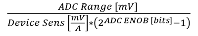
As an example, calculate the resolution of the ACS732KLATR-20AB-T at 1MHz bandwidth using a 5 V ADC with 11.5 effective number of bits. The ACS732 is specified with a noise density of 55 (µARMS)/√Hz.
Multiply this value by √(1MHz * π/2) to get a noise of 69 mARMS, which gives the resolution of the sensor output.
Next, calculate the ADC resolution where:
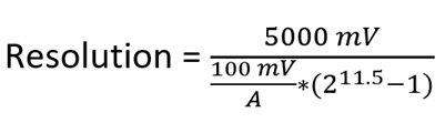
This results in an ADC resolution of 17 mA. When calculating the total resolution of the system, take the maximum of these two calculations, or in this case, 69 mA.
Low pass filtering of the Allegro current sensor output will decrease the noise but at the cost of device bandwidth. If a specific noise level or resolution is desired, solve for bandwidth (BW) in the following equation: desired noise = noise density * √(BW*π/2).
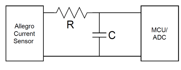
Next, pick R and C values that generate the desired bandwidth. The bandwidth of an RC filter is equal to 1 / (2*π*R*C). It is important to use an R value that is low enough to not affect the ADC reading. Because ADC’s generally have high input impedance, a value of around 1Kohm or less is typically acceptable.


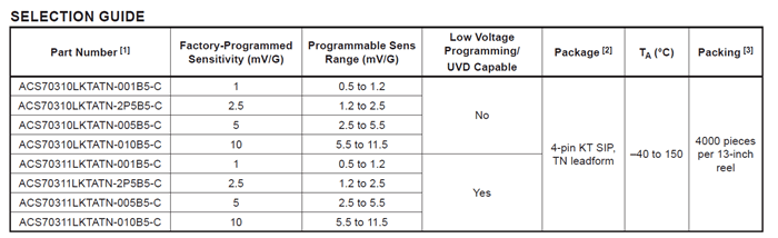
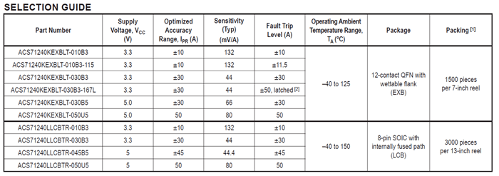
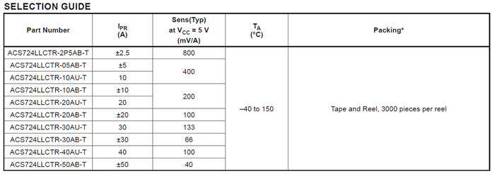
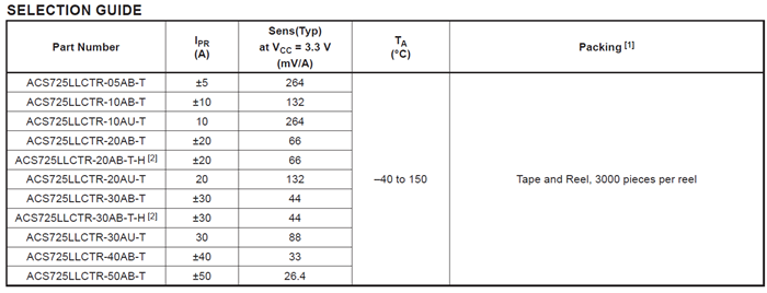
Listed in the datasheet for each device is a Selection Guide, typically located on page 2 or 3. While there is some variation from device to device in what is included in the device selection guide, some primary attributes of the selection guide are the part number, sensitivity (Sens), optimized current range (only applicable to integrated conductor sensors), operating temperature (TA), package type, and supply voltage (if the device has 5 V and 3.3 V variants). This table can be used as a guide when selection the current sensor for an application.
Examples:
Core based (ACS70310) Selection Guide from device datasheet:
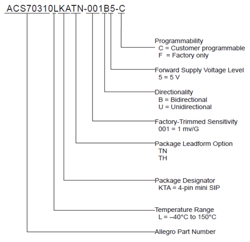
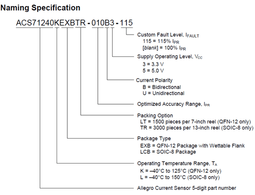
There are two basic Allegro current sensor naming schemes, one for integrated (ACS71240, ACS724, ACS37002, etc.) and one for core-based sensors (ACS70310, A1365, etc).
Common naming components to integrated and core-based sensors: Allegro current sensors begin with ACS (with the exception of legacy A1363/5/6/7), followed by a three to five digit part number. The part number is followed by a letter to indicate the operating temperature range of the sensor. The temperature range designation is followed by the package designator, which can be two/three digits. Following the package designation, integrated sensors then have a two letter designation for available packaging/shipping options and core-based sensors will have a two letter designation for the leadform option. Next, integrated sensors have a two/three digit current range value and the core-based sensors have the trimmed sensitivity value. This is then followed by the sensor’s directionality, bidirectional (B) or unidirectional (U). Next is the device’s nominal supply voltage level. Included at the end of the part name are custom features (custom fault level, set polarity, customer programmable, etc.). See the device specific datasheet for more information about the device’s part number. Note that legacy devices, like the ACS722/ACS723, ACS724/ACS725, and ACS732/ACS733, do not have a bidirectional or unidirectional designation in the name nor do they have a designation for nominal supply voltage. Different part numbers were made for 3.3 V and 5 V variants (i.e., the ACS724 is a 5 V device while the ACS725 is a 3.3 V device but these parts have identical functionality).
Examples of Naming Schemes:
Core Based (ACS70310):
Integrated (ACS71240):
Legacy Integrated (ACS724 vs. ACS725, note no supply voltage designation in the Selection Guide):
A min/max limit guarantees that no devices will be above or below the min/max value when leaving the Allegro factory. Typical values are mean ± 3 sigma. This means that 99.7% of devices will fall within the typical values and none will fall outside the min/max limits within the specified operating temperature range, input voltage, or any other test conditions.
It is also important to note that Sensitivity Error (ESENS) and Total Error (ETOT) are specified at a given current (typically the full-scale current, or half-scale current). Error results may vary with different applied currents. The main example of this is Total Output Error at lower currents. For example, if the full-scale range of a part is 20A and there is a 5% maximum Sensitivity Error and 1A maximum Offset Error, maximum Total Output Error = 20 A * (5% / 100) + 1 A = 2 A or 10% of the full-scale applied current of 20 A. At 5 A applied with the same sensitivity error and offset, Total Output Error = 5*(5% / 100) + 1 A = 1.25 A or 25% of the full-scale applied current.
Navigate to the Allegro Microsystems homepage. Allegro current sensor demo boards begin with the “ASEK” designation. For example, if a ASEK37800KMAC‐015B5‐SPI demo board is required to evaluate the ACS37800KMACTR-015B5-SPI, search ASEK37800 in “Check Stock” search bar on the top right corner of the Allegro homepage.

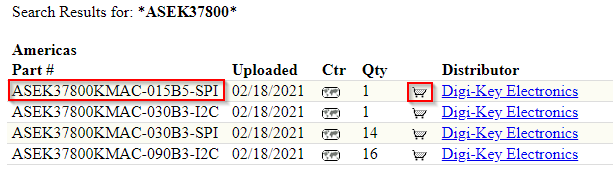
The search for “ASEK37800” will provide results for all available ASEK37800 demo boards. Click the Cart icon to be routed to the Digikey website for purchase.
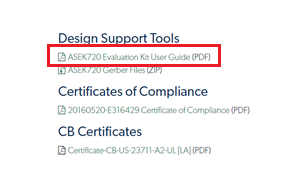
On the device home page, click the link for “Design Support Tools” as shown in the picture below:

If the demo board has a user guide it will be available in the Design Support Tools with a downloadable link as shown below:
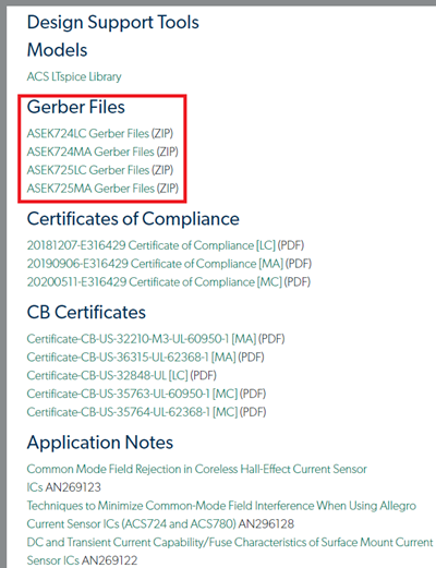
On the device homepage of each Allegro current sensor is a Design Support section, located near the bottom of the web page. Here, there is a zip file containing the Gerber files of the ASEK demo board for the device. Gerber files are files that contain information on each board layer of a PCB design.
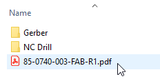
After unzipping the Gerber files folder, there will be a FAB document. This FAB document contains information about the demo board layout as well as information about copper thickness, PCB layer count, among of the demo board attributes.
In each device datasheet, there is a PCB layout and thermal application section that is specific to that device and package.
Related Application Notes:
Refer to Question 1 of the Design Support FAQ section to learn about mitigating stray fields.
On the specific Allegro current sensor device homepage, navigate to the “Part Number Specifications and Availability”. Select “View Data” on the desired gain option. The package weight is included in the “Materials Declaration Report”.
Also refer to Question 6 of the General Question section of the FAQ for more package information.
There are several ways to begin the product selection flow. The first would be based off the required isolation or package size. The following table provides an overview of the available packages (not including field sensors).
|
Package Descriptor |
SOICW-16 LA |
SOICW-16 MA |
SOICW-16 MC |
SOIC-8 LC1 |
SOIC-8 LC2 |
QFN-12 EXB |
7-pin PSOF LR |
5-pin CB |
|
Picture |
|
|
|
|
|
|
|
|
|
Dimension |
10.3x10.3mm |
10.3x10.3mm |
11.3x13mm |
4.9x6mm |
4.9x6mm |
3x3mm |
6.4x6.4mm |
14x22mm |
|
Conductor Resistance |
0.85 mΩ |
0.85 mΩ |
0.27 mΩ |
1.2 mΩ |
0.65 mΩ |
0.6 mΩ |
0.2 mΩ |
0.1 mΩ |
|
Dielectric Strength |
RMS3600 V |
RMS5000 V |
RMS5000 V |
RMS2400 V |
RMS2400 V |
NA |
NA |
RMS4800 V |
|
Working Voltage |
DC870 V RMS616 V |
DC1550V RMS1097 V |
DC1618 V RMS1144 V |
DC420 V RMS297 V |
DC420 V RMS297 V |
DC100 V RMS70 V |
DC100 V RMS70 V |
DC1358 V RMS700 V |
The other product selection flow may begin with the required current sensing level. Allegro has landing pages for various current sensing levels including:
The Current Sensors Innovations also highlights the benefits of the different product families.
When debugging stray magnetic fields, check to see if the sensor is single or dual hall technology by checking the functional block diagram on the device specific datasheet.
Single Hall and Stray Fields:
Because Allegro current sensors use the Hall Effect to measure current, any additional magnetic field seen at the hall element outside of the current being measured will affect the output of the sensor. These additional magnetic fields are generally called stray or common magnetic fields. The most common cause for stray magnetic fields is the presence of a high current trace or wire near the current sensor. To approximate error caused by a current carrying wire, model the magnetic field of the trace as an infinite wire where B = µ* (I / (2π×d)).
B is the magnetic field in Gauss (G), µ is the permeability of free space in G equal to 4π*0.001, I is the current in amps, and d is the distance in meters of the line from a point on the wire to the hall element perpendicular to the wire. Once the magnetic field is known, multiply by the magnetic coupling factor [G/A] (provided in most datasheets) which will result in an absolute error in amps. Once error is estimated, testing can be performed by removing the stray field generating wire or trace and retesting the sensor output. Another solution if the trace or wire cannot be removed is to pull the sensor off the board and wire the part off the PCB away from the suspected current carrying wire. Lastly, shielding can be utilized by placing a ferrous material around the sensor to block the stray field.
This application note describes in more detail the effects of magnetic field interference and shielding.
Dual Hall and Stray Fields:
Allegro also offers sensors with dual hall elements to mitigate stray field error. Two Hall elements are used differentially and placed on opposite sides of the current loop. This allows the common magnetic field to be removed allowing output voltage to be significantly unaffected by the common field. Although dual hall elements minimize stray field error, they do not entirely eliminate the potential of error induced by stray field. The same testing/mitigation techniques in the previous paragraph can also be used when debugging dual hall sensors.
This application note explains in more detail how to estimate and mitigate common magnetic field when using sensors with dual hall elements.
The following is a check list to follow to verify the proper output of an Allegro current sensor:
Other potential issues include noise (refer to the Noise section of the FAQ) and stray magnetic field (refer to the Design Support Section of the FAQ).
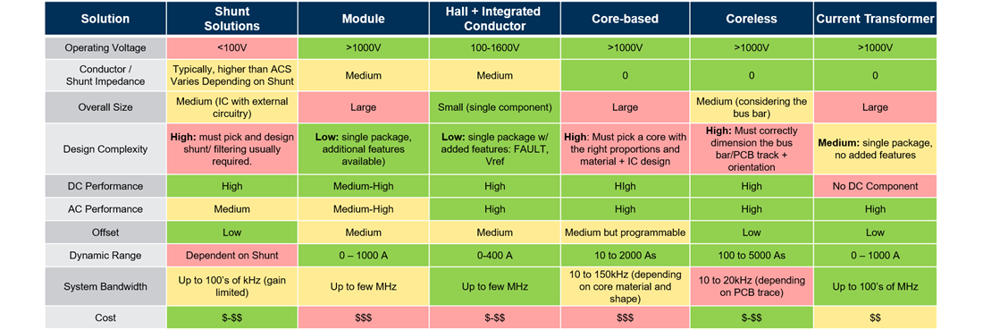
There are many ways to measure current in a system, but the following table highlights and compares the main current sensing solutions:
The ASEK20 is a device used to program and evaluate customer programable Allegro current sensors (the ASEK20 can be used for angle position, linear position, and digital position sensors). The ASEK20 is used in combination with the device specific daughterboard (which are available separately from the ASEK20). The ASEK20 is a benchtop validation and programming tool useful in characterizing and understanding the performance of Allegro current sensors. The ASEK20 is also useful in calibrating Allegro current sensors in the field. Device specific software applications can be found on Allegro’s Software Portal.
Customer Programable Allegro Current Sensors that can be used with the ASEK20: