Monolithic Magnetic Hall Sensor ICs Using Dynamic Quadrature Offset Cancellation
By Alberto Bilotti, Life Senior Member, IEEE, Gerardo Monreal, and Ravi Vig
Abstract—The offset voltage, and its temperature drift and production spread, which generally degrades the zero-level stability and reproducibility of magnetic Hall sensor ICs, can be reduced using a single Hall plate and switching means for periodic permutation of the supply and output contact pairs. The present work describes a chopper-based 5-V monolithic linear Hall sensor IC with a ±0.1 T full scale where this dynamic plate offset cancellation technique has been employed together with a cost-effective signal conditioner. The device was integrated using a 2-µm conventional BiCMOS process and the final chip, measuring 1.5 × 1.5 mm, shows, after packaging in a 3-pin plastic package, a residual offset with a production spread and a temperature-induced drift five to ten times smaller than in currently used multiplate DC quadrature cancellation approaches. The device does not require external components and provides an output free of HF residues.
Index Terms—BiCMOS analog integrated circuits, choppers, Hall devices/effect, microsensors, monolithic integrated circuits.
I. INTRODUCTION
MONOLITHIC magnetic sensor ICs generally use Si Hall elements which are integrated simply with the amplifier or signal-conditioner circuits required for amplification or processing the relatively low voltages generated. The Hall effect, its characteristics, applications, etc., have been extensively dealt with in the literature [1]−[3]. An excellent review with many references can be found in Baltes' and Popovic's work.
The simplest Hall element uses a square plate made, for example, of an Epi-pocket in a bipolar or BiCMOS process with two pairs of orthogonally-oriented contacts, as shown in Fig.1. When a supply voltage Vs is applied across one pair of contacts, for example a, c, a magnetic flux density B normal to the plate generates a voltage VH across the other pair b, d, such that
where Sv is the Hall element sensitivity per unit supply voltage. The sensitivity given by VH ⁄B × Vs [T-1], where T (tesla; 1 T = 1 × 10⁴gauss) is the meter-kilogram-second (mks) unit for magnetic flux density (induction), is approximately a constant parameter, depending only on the Si layer mobility and the plate and contact geometries. Typical values of Sv range between 0.04 and 0.08 T-1, which means, for a typical 5-V supply and minimum magnetic flux density of 1 mT, output voltages of 200 to 400 µV.
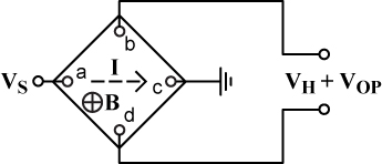
Fig. 1. Basic Hall plate.
In all DC applications, the minimum magnetic flux density capable of being accurately measured by such plates depends on the offset voltage Vop appearing at the plate output contacts for B = 0. The plate, from an electrical point of view, will show unavoidable imbalances due to resistance gradients, geometrical asymmetries [4], piezoresistive effects [5], [6], etc., generating a nonnegligible offset voltage. As the plate offset Vop is relatively large—it may range from 0.5 to 5 mV for a 5-V supply and is temperature-, supply voltage-, and stress-dependent—efforts have been made for cancelling or minimizing its effects.
Offset cancellation cannot be performed by such switching techniques as those used in amplifiers, as there is no available state where Vop could be isolated from VH except cutting off the magnetic field, which is certainly a nonviable proposal.
Noting that, from a DC point of view, the Hall plate can be viewed as a distributed resistive Wheatstone bridge, most present commercial Hall sensor ICs cancel the offset by using two or more appropriately interconnected plates where the electrical current direction is 90° rotated from one plate to the other [7]. If the imbalance source remains invariant and fixed in the solid space, the offsets of any pair of plates will be equal but of opposite polarity, achieving the desired cancellation. On the other hand, the useful signal of the multiplate arrangement remains equal to that of a single plate.
Alternatively, the use of only one plate while generating the quadrature states by periodic supply and output contact permutations has been proposed [8], [9]. Although this dynamic offset cancellation technique requires a more complicated signal conditioner following the Hall switched-plate, it has the advantage of reducing the residual offset and its production spread as compared with multiplate sensor ICs. In the last case, the zero-level deviations are degraded due to plate offset mismatches between physically different plates, these mismatches being mostly generated by the plastic package temperature-dependent built-in stresses.
This work describes 5-V BiCMOS monolithic linear Hall sensor ICs using the dynamic offset cancellation technique, where the various functions required for recovering the useful signal and cancelling the offset are performed by a cost-effective signal conditioner.
A BiCMOS technology was preferred in order to have simple high-gain open-loop amplifiers with low offset, accurate temperature-programming circuits, as well as a low-cost high-output current sourcing capability.
II. THE SWITCHED HALL PLATE
The simplest dynamic offset cancellation technique uses a single square plate with four contacts where the quadrature states are generated by periodically connecting the supply voltage and supply conditioner input to one pair of contacts or to the other, as shown in Fig. 2. Each state, which we shall call from now on the 0° state or the 90° state, is defined by the complementary clocks CLK1 and CLK1_bar, respectively.
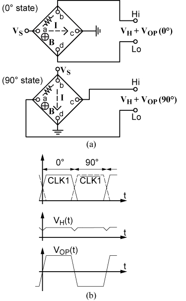
Fig. 2. (a) In a dynamic offset cancellation technique, the current flowing through the plate is periodically switched from the 0° to the 90° direction and vice versa. (b) Clock, Hall voltage, and plate offset waveforms.
Assuming B = 0 and an ideal Wheatstone bridge model for the Hall plate, the voltages appearing at the output contacts are the plate offsets Vop(0°) and Vop(90°) which are equal in magnitude but have opposite polarities. This can be verified in a very simple way as follows. Assume that an imbalance, for example due to a stress pattern, occurs such that the region between contacts a and b shows a resistivity smaller than the rest of the plate (dotted resistor in Fig. 2), and that this situation does not change when changing states. Then, the offsets developed at each state have the same magnitude but opposite polarities, as the same imbalance occurs in adjacent branches of the equivalent bridge network (the Hi terminal will be more positive than the Lo terminal in the 0° state but more negative in the 90° state).
For B ≠ 0, as the supply and output connections rotate in the same direction, VH keeps its polarity unchanged, making VH invariant. This characteristic of VH derives from the antireciprocal property of a symmetrical Hall plate.
There appears, therefore, a simple way to discriminate the offset from the useful signal and further cancelling the offset by appropriate signal conditioning. Although in Fig. 2, VH is quasi-constant and Vop an alternating square wave, waveforms can be interchanged if desired by interchanging output contacts a and c during the 90° state.
As an ideally perfect cancellation is never possible, there is in practice a residual plate offset Vop (r) defined as
where absolute values have been preferred for emphasizing the polarity reversals occurring during further signal processing. Depending on the fabrication process, the Hall plate geometry and crystallographic orientation, and the residual wafer and package stresses, Vop(r) may range between 50 and 500 µV for a 5-V supply.
DC measurement data of a quadrature cancellation on a single plate, either in an Epi plate [9] or in an MOS channel "plate" [10], showed an appreciable improvement as compared to the conventional multiplate approach. For reducing Vop(r) these measurements were performed in plates using four pairs of contacts distributed around the periphery of a circular plate as in a "spinning" Hall cell [9]. In this case, multiplexed addition of all possible offsets for improving cancellation would require eight switching states per cycle.
For simplifying purposes and reducing chip area, the simplest approach of the Epi plate with two pairs of contacts and two phases per cycle as shown in Fig. 2 was chosen for our monolithic sensor IC.
The maximum allowable plate switching frequency depends on the plate voltage settling time after each commutation transition. Note that, for example, after the transition from the 0° state to the 90° state, the voltage Va at contact a in Fig. 2 has to decay from Vs to Vs ⁄ 2, and Vc has to increase from zero to Vs ⁄ 2 (while voltages at d and b have to decay to ground and increase to Vs, respectively). This requires a rearrangement of charges stored in the Epi-Sub reversed-biased junction and therefore, a certain time for voltages to settle down into the final value Vs ⁄ 2, after which the Hall output voltage will be valid and ready to be processed, as shown in Fig. 3.
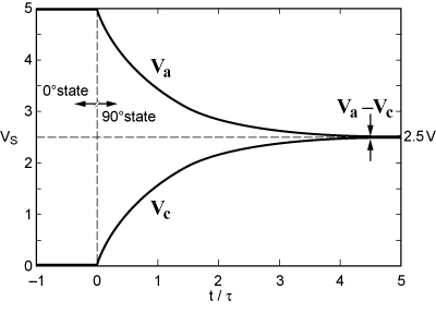
Fig. 3. 0° state to 90° state Hall plate switching transient where Va and Vc are the voltages at contacts a and c in Fig.2.
Switching measurements, of a Hall plate built on a square Epi layer that was 2 Ω-cm, 5.5 µm thick, with 3 kΩ resistance between diagonal-opposite facing contacts, showed that the Hall voltage will be valid only after ≈600 ns have elapsed from the plate commutation transition. Taking into account component tolerances and the fact that additional sample pulses must be included in each phase, a maximum plate switching frequency of 200 kHz was found. As long as the switching frequency remains below this limit, the switching frequency is not critical for the system operation, simplifying, therefore, the implementation of the clock circuitry.
Even if there would be a residual voltage due to an excessive settling time, this voltage would remain invariant during both states, just as the true offset does, and therefore would be cancelled out. This has not been exploited further as it requires a very accurate and more costly CLK generator.
Fig. 4 shows the actual switched-plate arrangement used in the monolithic sensor IC where the four single-pole double-throw (SPDT) switches required for the contact permutation were implemented with MOS transistors. The plate contact interconnections follow the basic scheme of Fig. 2 except for an interchange of the output terminals during the 90° state. With this arrangement, at each change of state, VH changes polarity and Vop remains quasi-constant, in such a way that VoA, the DC input-referred offset of amplifier A1, will become indistinguishable from Vop, and the Hall plate and the input amplifier offsets will be simultaneously processed and cancelled by the signal conditioner.
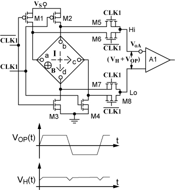
Fig. 4. Switched Hall plate. When the CLK1 signal is high, current flows between a and c (0° state) and when CLK_bar is high, current flows between b and d (90° state).
Thus, the A1 offset is cancelled at no cost, avoiding the extra hardware required to perform the same function by other techniques such as autozero, signal conditioning (SC), etc.
The input voltages to the ideal amplifier A1 become
Vi (90°) = −VH + |Vop (90°)| + |VoA | during 90° state. (3b)
For avoiding degrading Vop(r) through eventual mismatchings between the supply voltages effectively applied to the plate during each phase, transistors M1 through M4 were properly sized so as to keep their on-voltage drop below 100 mV.
Taking into account that the total offset Vop + VoA must be amplified without distortion by A1, dynamic range considerations require minimizing VoA, therefore suggesting the use of a low-offset differential bipolar input stage. In this case, base input currents Ib flowing through MOS switches M5 through M8 may generate a residual offset VoI (r) additional to that given by equation 2. Assuming ΔIb «Ib, straightforward calculation gives
where
As A1 uses a conventional base current cancellation circuitry, VoI (r) is smaller than 2 µV and, therefore, can be fully neglected as compared to Vop(r).
III. SIGNAL CONDITIONER
Fig. 5 is a simplified block diagram of the complete linear Hall device, where the previously described switched-Hall plate is represented by block SWP. Note that for zero offset and B = 0, the output amplifier A2 has its quiescent output voltage, VQoi, defining the sensor zero level, at Vs ⁄ 2. The signal conditioner operates as a quasi-chopped amplifier where the first pair of cross-coupled switches are built in the switched Hall plate, and where the second pair of switches plus the conventional low-pass (LP) filter have been substituted by sample and hold (S/H) and adding functions, as described next.
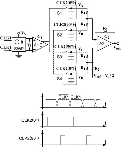
Fig. 5. Hall device block diagram.
The differential-differential amplifier A1 amplifies G1 times the signal Vi comprising the quasi-DC offset voltage plus the alternating useful Hall signal generated by the switched Hall plate. In conventional chopper amplifiers, the useful signal is recovered and the offset cancelled by additional switches after the amplifier, that inverts again the composite signal polarity, and by further LP filtering.
In this application, as at low magnetic flux density levels, the Vop ⁄ VH ratio may attain high values, a costly multiple-pole LP filter is required for reducing the residual AC ripple. For example, for insuring a maximum peak-to-peak ripple of 20% in the worst case of Vop = 10 mV and VH = 0.25 mV, the fundamental component of the square-shaped offset voltage must be attenuated 52 dB. When operating at a clock frequency of 150 kHz with a bandwidth of 34 kHz, a four-pole LP filter is required. Besides, the useful signal may be corrupted by DC components, generated by the large pulses occurring at each plate switching, that may go through the LP filter.
The problem was circumvented by using, at the outputs of A1, two S/H circuits S1 and S2, which are clocked by narrow pulses CLK2(0°) and CLK2(90°), respectively. This occurred during the 0° and 90° states, once the required delay for the plate commutation transients to die out had elapsed [11].
Assuming an ideal S/H function, the offset voltages at the S/H outputs are DC signals, and there is no need any more to further filter out the otherwise high offset AC ripple, relaxing the output LP filtering requirements. Also, the synchronous sampling of the signal by the samplers when the signal is free of spurious pulses improves the accuracy of the signal recovery process, particularly at low levels.
As far as the output noise is concerned, this is mainly due to the thermal noise of the Hall plate resistance. When compared to a conventional chopper, the S/H function in the present approach produces a higher noise power spectral density at low frequencies due to a higher "fold-back" of HF noise components into the baseband.
Recalling equations 3a and 3b, assuming ideal S/H functions and noting that the S/H inputs are complementary outputs of A1, the S/H outputs VA and VB are, neglecting common mode (CM) signals, DC voltages given by
VB = ½G1 [VH − |Vop (90°)| − |VoA | ]. (7)
Adding these two DC voltages, by means of the inverting two-input summing op-amp A2, with gain G2 = − R2 ⁄ R1, and then inserting the quiescent output voltage VQo, produces, neglecting A2 offset contributions, the output
= VQoi + ½G1 × G2 × Vop(r) + G1 × G2 × VH (8a)
or
where VQoi = Vref = Vs ⁄ 2 is the ideal quiescent output voltage for Vop(r) = 0 and VQo the actual quiescent output voltage. Note that the amplification ½G1 × G2 of the undesirable residual offset is half that of the useful signal.
Apart from Vop(r), there are other components that remain uncancelled and that will shift VQo from its ideal value, such as offsets due to the feedback amplifier, resistor networks, and S/H mismatchings, etc. As the total offset can be nulled at one temperature by any wafer-trimming technique, the offset drift with temperature and its production spread, particularly due to package-induced stresses, remain the most critical sensor IC issues.
For reducing the effects of S/H imperfections such as charge feedthrough, droop, nonlinearity, etc., the final monolithic sensor IC uses a fully differential S/H configuration comprising four S/H circuits S1 to S4 and a summing feedback difference output amplifier, as shown with dotted lines in Fig.5. In this way, the signal is differentially processed all along the whole system.
- Amplifier A1 is an open-loop amplifier with a bipolar input differential stage using differential resistive loads, as shown in Fig. 6. The quiescent output voltage is stabilized by means of a negative feedback loop comprising Q5, Q6, M5, M6, and M7. As compared to a closed-loop amplifier, the open-loop approach does not require stability capacitors, avoiding any settling time degradation due to slew rate limitations.
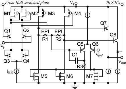
Fig. 6. First amplifier A1.
Care was exercised to avoid undesirable saturation effects increasing the amplifier settling time beyond the plate settling time previously discussed, decreasing the maximum allowable switching frequency. For this, a gain-killer circuit comprising a simple gated CMOS pass transistor that short-circuits the bases of Q7 and Q8 during the Hall plate switching transitions was incorporated into the amplifier.
Although maximum gain is a desirable feature for reducing the effect of post-amplifier offsets as compared to Vop(r), the input stage was emitter-degenerated for increasing the linear input range. The linearity, for the maximum input swing, is better than 99.9%.
Diodes were used for emitter degeneration for keeping the stage transconductance proportional to IEE ⁄ Vt, allowing simple linear adjustment of IEE. By using a PTAT (proportional to absolute temperature) emitter current bias, the stage transconductance becomes temperature independent, while the Epi load resistors, similar to the Epi plate, make the amplifier gain vary with temperature as (mobility)–1 cancelling the Hall sensitivity mobility dependance and reducing the sensor IC sensitivity variations with temperature.
In any chopping amplifier the higher the chopping frequency the smaller the filter capacitors. Consequently, for reducing the chip area, a chopping frequency of 170 kHz, close to the maximum allowed by the Hall plate transition times, was chosen.
The amplifier has a typical gain of 30×, a –3 dB frequency of 4 MHz, and a 0.01% settling time of 400 ns. The offset square wave signal is therefore amplified with negligible frequency distortion.
- The S/H function is performed at signal levels G1 times higher than the input level, making the undesirable effects of S/H imperfections less noticeable, these imperfections being further cancelled by the differential S/H arrangement previously mentioned.
For cost-reduction purposes, the S/H elements were implemented as open-loop circuits, the grounded holding capacitor being sensed by a high-beta lateral-PNP (LPNP) bipolar transistor, Q3 as shown in Fig. 7. Transistors Q1, Q2, and Q4 help reducing Q3 base current, reducing therefore the droop.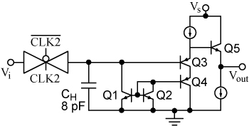
Fig. 7. S/H circuit configuration.
- The output rail-to-rail feedback amplifier is a rather conventional op-amp. It has a typical gain of 6× and is capable of sourcing a maximum of 2 mA into the load. An internal feedback capacitor of 20 pF stabilizes the loop and limits the bandwidth to ≈30 kHz. This post-sampling narrowbanding reduces the typical output staircase ripple at high operating frequencies and the output white noise.
IV. MONOLITHIC IMPLEMENTATION
A ±0.1 T full scale linear Hall device using dynamic offset cancellation and the basic circuits previously described was implemented in a monolithic IC using a 2–µm BiCMOS process. The supply voltage is 5 V ±10%, and no internal voltage regulator is used because in many applications of linear sensor ICs, particularly in the automotive environment, the sensitivity should preferably be proportional to the supply voltage. This ratiometric feature allows cascading the sensor IC output directly to an A-to-D converter fed from the same supply. The device uses no external components, is packaged in a 3–pin plastic package, and operates within a –40°C to 150°C temperature range.
In order to reduce the production spread of the magnetic sensitivity, gain G1 is trimmed by adjusting IEE (Fig. 6) with a 4-bit binary-weighted fuse-link network. Similarly, the total circuit residual offset, affecting the quiescent output voltage, is trimmed out by another fuse-link network. Both adjustments are performed at the wafer level at one single reference temperature.
The chip, measuring 1.5 × 1.5 mm, is shown in Fig. 8. The Hall Epi plate, measuring 160 × 160 µm, is located at the chip geometric center. The three clock signals CLK1, CLK2(0°), and CLK2(90°) are derived from a master oscillator, and are generated on-chip.
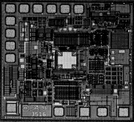
Fig. 8. Microphotograph of the Hall sensor IC die. Die size is 1.5 × 1.5 mm.
As low-level analog and 5-V digital signals share the same chip, layout precautions were taken for minimizing digital feedthrough into sensitive areas, therefore minimizing any residual output digital noise.
V. EXPERIMENTAL RESULTS
Table I gives the measured typical characteristics of the final packaged Hall device at TA = 25°C.
TABLE I
| Vsupply | 5 V |
| Isupply | 7 mA |
| Iout(max) | 2 mA |
| Sensitivity | 25 V ⁄ T |
| Full scale | ±100 mT |
| Quiescent output voltage | 2.5 V |
| Equivalent magnetic offset | 0.5 mT |
| Linearity | 99.9% |
| Output noise* | 1 mVrms |
| Bandwidth | 30 kHz |
*Vsupply lead decoupled with a 0.1 µF capacitor.
Fig. 9 shows the measured Hall device transfer function Vout = ƒ(B). The linearity, measured as an approximation to the best fit to an ideal straight line, amounts to 99.9%.
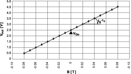
Fig. 9. Measured transfer function Vout = ƒ(B) at 25°C.
Figs. 10 and 11 show the performance of VQo, and total sensitivity S, as functions of temperature within the full ambient temperature range –40°C to 150°C.
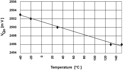
Fig. 10. Typical quiescent output voltage variation with temperature.
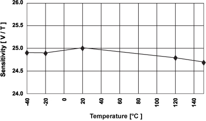
Fig. 11. Typical sensitivity variation with temperature.
The total output residual offset can be derived by measuring the difference between VQo and Vref (see Fig. 5) at the wafer level. Measurements at 25°C show offsets ranging from 5 to 20 mV, i.e., from 0.2 to 0.8 mT. The 2.5-V wafer-trimmed value of VQo at 25°C remains practically unchanged after packaging. The VQo deviation at other temperatures from its reference value at 25°C, shown in Fig. 10, represents a temperature-induced drift in the offset voltage. The typical total drift for the full temperature range is ≈7 mV, equivalent to a magnetic field of ≈0.3 mT. Preliminary production data show a 3σ spread in the quiescent output voltage of only ±10 mV. When using multiplate static offset cancellation techniques, these deviations, mainly caused by package-induced stresses, can be much larger, degrading the sensor IC zero reference stability.
Fig. 12 shows the sensitivity variation with the supply voltage.
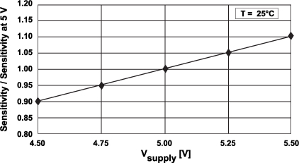
Fig. 12. Typical sensitivity variation with supply voltage.
Fig. 13 gives the Hall device output for B = 0, the oscilloscope photo being taken with the timebase synchronized to the clock frequency. It shows that due to the on-chip S/H filtering action, the CLK frequency residue is negligible and the main HF components left at the output are only those due to the random noise generated by the Hall plate resistance. Consequently, no external LP filter is required. If desired, the output noise can be further reduced by additional external LP filtering at the output, reducing at the same time the system bandwidth.
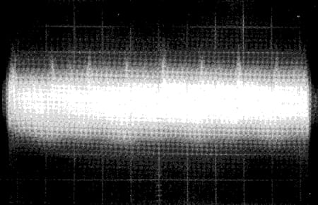
Fig. 13. System output noise, measured with a 0.1 µF decoupling capacitor at the Vsupply lead. Vertical sensitivity 2 mV ⁄ div. Horizontal sensitivity 1 µs ⁄ div. Timebase synchronized to CLK frequency.
Finally, Fig. 14 shows the sensor IC output voltage for a sinusoidal magnetic flux density.
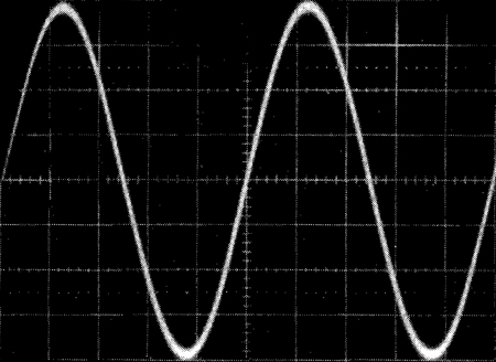
Fig. 14. Output waveform for a 400 Hz sinusoidal magnetic flux density. Vertical sensitivity 50 mV ⁄ div. Horizontal sensitivity 0.5 ms ⁄ div. Magnetic flux density amplitude: 8 mT.
VI. CONCLUSIONS
The described ±0.1 T monolithic Hall linear sensor IC using dynamic switching with two pairs of contacts and two switching states appears to be an attractive cost-effective option for reducing the sensor IC offset drift with temperature and the offset reproducibility. As the offset itself is simply trimmed out at the wafer level at one reference temperature, the offset drift with temperature and its reproducibility particularly in plastic-packaged devices becomes the most crucial issue affecting the sensor IC zero stability. In this respect, the present device, after plastic packaging, shows a zero-level stability that compares very favorably with commonly used multiplate DC approaches.
The relatively small chip size proves that this technique can be cost-effective, particularly when recovery of the useful signal and offset cancellation are performed by S/H circuits, substituting for the large-footprint LP filter of a conventional chopper used otherwise. The S/H circuits also help in ignoring the large commutation transients occurring during plate switching, providing an accurate and smooth linear transfer function at very low levels.
Although digital and low-level analog signals share the same chip, the spurious CLK noise developed at the output is almost negligible as compared to the random noise due to the Hall plate resistance.
As suggested in the literature, a higher number of plate contact pairs and switching phases per cycle seems to improve the Hall plate offset cancellation. Certainly this option could be an interesting challenge, requiring a more refined signal-conditioning circuitry operating at higher frequencies and showing an offset sufficiently small not to compromise the advantages gained by the more sophisticated plate switching.
Although the present work deals with linear Hall sensor ICs, the same techniques could be used for implementing the commonly used digital sensor ICs with "operate" and "release" switching levels. In this case, the improvements in the zero level deviations achieved in the present linear sensor ICs will translate into better reproducibility and temperature stability of the switching thresholds.
ACKNOWLEDGMENT
The authors gratefully acknowledge the useful discussions with J. Higgs, K. Scheller, and J. Towne, and the extensive experimental work performed by A. Gibbs, all with Allegro MicroSystems, LLC
REFERENCES
[1] C. L. Chien and C. R. Westgate, The Hall Effect and Its Applications. New York, NY: Plenum, 1980.
[2] H. P. Baltes and R. S. Popovic, "Integrated semiconductor magnetic field sensors," Proc. IEEE, vol. 74, pp. 1107-1132, Aug. 1986.
[3] G. S. Randhawa, "Monolithic integrated Hall devices in silicon circuits," Microelectron. J., vol. 12, no. 6, pp. 24-29, 1981.
[4] G. Bjorklund, "Improved design of Hall plates for integrated circuits," IEEE Trans. Electron Devices, vol. ED-25, pp. 541-544, May 1978.
[5] Y. Kanda and M. Migitaka, "Effect of mechanical stress on the offset voltage of Hall devices in Si IC, " Phys. Status Solidi (a), vol. 35, pp. K115-K118, 1976.
[6] ----------, "Design considerations for Hall devices in Si IC," Phys. Status Solidi (a), vol. 38, pp. K41-K44, 1976.
[7] J. T. Maupin and M. L. Geske, "The Hall effect in silicon circuits," in The Hall Effect and its Applications, C. L. Chien and C. R. Westgate, Eds. New York, NY: Plenum, 1980.
[8] P. Daniil and E. Cohen, "Low field Hall effect magnetometry," J. Appl. Phys., vol. 53, no. 11, pp. 8257-8259, Nov. 1982.
[9] P. J. Munter, "A low offset spinning-current Hall plate," Sensors and Actuators, vols. A21-A23, pp. 743-746, 1990.
[10] R. Gottfried-Gottfried, "Ein CMOS Hall Sensor mit 8 Kontakten zur Anwendung des Principes der Stromrichtungsumkehr," Sensor 93 Kongressband V, pp. 203-210.
[11] U.S. Patent 08 569 814.

Alberto Bilotti (S'45–A'48–SM'65–LS'91) received the degree in electrical engineering from La Plata University, Argentina, in 1948.
He worked with Philips, Argentina for seven years, IBM, France for five years, and Sprague Electric Co., USA, for three years. His main activities were design of color televsions, advanced development in memories and PBXs, and design of analog ICs, respectively. From 1975 to 1985, he was responsible for R&D in Fate Computer Co., Argentina. At present, he is a consultant in the area of analog-digital ICs, smart power ICs, and magnetic sensors.

Gerardo Monreal was born in Buenos Aires, Argentina, in 1968. He received the degree in electronic engineering from Universidad de Buenos Aires, Argentina, in 1994.
He started working on neural networks at the Universidad de Buenos Aires. In 1992, he joined Electrónica Bilotti where he serves as an IC Design Engineer. Currently, his works concern analog-digital ICs and magnetic smart sensor ICs.

Ravi Vig was born in Mumbai, India. He received the B.S. (EE) degree from Rutgers University, New Brunswick, NJ, in 1982 and the M.S. (EE) degree from Dartmouth College, Hannover, NH, in 1984.
He has worked at Sprague Electric and then Allegro MicroSystems Inc., Worcester, MA, since October 1984, as an IC Design Engineer and later as Design Manager for Hall effect integrated circuit products. His activities have included high-temperature Hall sensor ICs, multiplexed sensor ICs, and self-calibrating gear sensor ICs. He has also worked as the Strategic Marketing Manager for Automotive Products. He currently holds the position of Vice President, Business Development at Allegro MicroSystems, LLC
Manuscript received July 26, 1996; revised November 28, 1996. This work was supported by Allegro MicroSystems, LLC, Worcester, MA.
A. Bilotti and G. Monreal are with Electrónica Bilotti, Olivos 1636, Argentina.
R. Vig is with Allegro MicroSystems, LLC, Worcester, MA, USA.
Publisher Item Identifier S 0018-9200(97)03841-9. 0018-9200/97$10.00 © 1997, IEEE
The products described here are the A3515xUA and A3516xUA, ratiometric, linear Hall-effect sensor ICs for high-temperature operation.
This paper was originally published in the IEEE Journal of Solid-State Circuits, Vol. 32, No. 6, June 1997. Reprinted by permission.
STP97-10