ACS758 Current Sensor ICs Frequently Asked Questions

The differences are the output sensitivities (in mV/A) of each version and their operating temperature ranges. Operating temperatures are also related to maximum current ranges.
Externally, the packages are identical and have the same footprint. Internally, the CB package leadframe has greater cross-sectional area where the conductor passes the Hall-effect device. As a result, the CB package conductor has a resistance of only 100 µΩ, versus 130 µΩ for the CA package. In addition, the CB core is made of laminated steel and has a much higher saturation point (at higher temperature) than the ferrite core inside of the CA package.
Yes. The ACS758 family uses Hall-effect technology, which is capable of sensing electrical currents having both DC and AC components. As the datasheet states, the bandwidth of the ACS758 is 120 kHz typical. There may be phase lag and amplitude attenuation of the output for AC currents with frequency content greater than 120 kHz. For transient current signals, the response time is ≈4 µs.
No, the maximum current in the sensing range of the ACS758 is an absolute current of 200 A. The magnetic circuit within the ACS758 package will not provide a linear output above field levels generated by 200 A.
This feature is particularly valuable when using the ACS758 with an analog-to-digital converter. A/D converters typically derive their LSB from a reference voltage input. If the reference voltage varies, the LSB will vary proportionally. The ratiometric feature of the ACS758 means its gain and offsets are proportional to its supply voltage, VCC. If the reference voltage and the supply voltage for the ACS758 are derived from the same source, the ACS758 and the A/D converter will both track those variations, and such variations will not be a source of error in the analog-to-digital conversion of the ACS758 output. Figure 1 is a plot of primary current, IP, versus output voltage, VOUT, of the ACS758-100A when varying VCC. The offset and sensitivity levels shift proportionally with VCC. For example, when VCC = 5.5 V, the 0 A output is 5.5 / 2 = 2.75 V nominal, and the sensitivity is 22 mV/A nominal.
  figure 1


Figure 1. ACS758-100A VOUT versus IP at various VCC 
Allegro recommends the use of a 0.1 µF bypass capacitor between the VCC pin and the GND pin. The capacitor should be located as close as practical to the ACS758 package body.
No, the ACS758 sensitivity and 0-ampere (quiescent) voltage level are programmed at the factory.

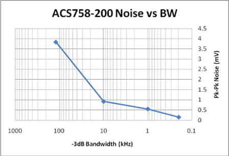
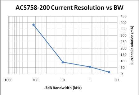
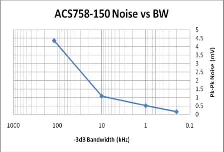
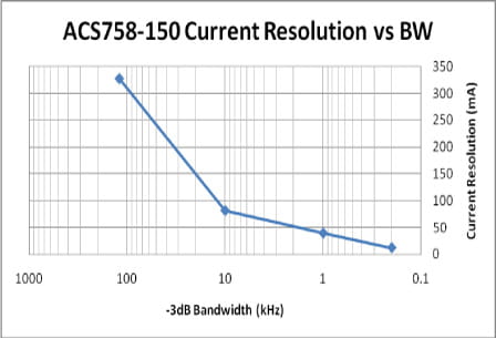
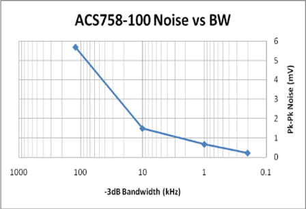
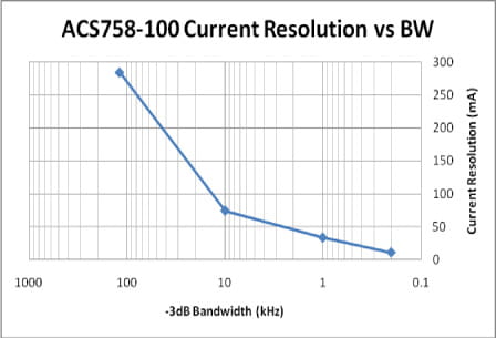
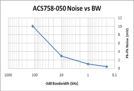
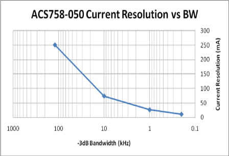
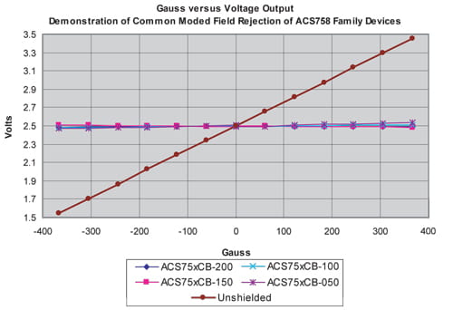
The current resolution of the ACS758 family of current sensor ICs is limited by the noise floor of the device output signal. For example, the ACS758-050 version can resolve a change in current level of about 250 mA, at 25°C, through its primary conductor leads. The 200 A version can resolve approximately 380 mA. At these levels, the amount of magnetic field coupled into the linear Hall-effect IC is just above its noise floor. Resolution can be improved significantly by filtering the output of the ACS758 for applications requiring lower bandwidth. Table 1 lists the noise levels, and hence current resolutions, at various bandwidths. Filtering was accomplished with a simple, first order RC filter. Note the related graphs, figures 2 through 5, which provide a better understanding of the device output resolution that can be achieved through filtering.

Table 1. ACS758 Noise Level and Current Resolution versus Bandwidth

Device Bandwidth -3 dB
(kHz)
Noise
(mVp-p)
Current Resolution
(mA) (% of full scale)
ACS758-200B 120 3.84 384 0.192
10 0.92 92 0.046
1 0.55 55 0.028
0.2 0.15 15 0.008
ACS758-150B 120 4.36 328 0.219
10 1.08 81 0.046
1 0.52 39 0.026
0.2 0.16 12 0.008
ACS758-100B 120 5.69 285 0.285
10 1.49 75 0.075
1 0.67 34 0.034
0.2 0.22 11 0.011
ACS758-50B 120 10.03 251 0.502
10 2.95 74 0.148
1 1.05 26 0.053
0.2 0.43 11 0.022 


figure 2a
Figure 2A 

figure 2b
Figure 2B 


figure 3a
Figure 3A 


figure 3b
Figure 3B 


figure 4a
Figure 4A 


figure 4b
Figure 4B 


figure 5a
Figure 5A 


figure 5b
Figure 5B 

Typical ESD tolerance is 6 kV human body model, 600 V machine model.
In order to safely conduct 200 A currents, the power leadframe in the ACS758 has been constructed with a relatively heavy gauge. Because of this heavy gauge, the terminal leads are not very flexible. If the ACS758 is surface-mounted, small amounts of board flex, or the action over time of thermal expansion and contraction, could potentially break the IC off the board. Allegro does not recommend surface mount assembly of this device.
To ensure a robust joint to the board, Allegro recommends adding a ring of through-holes in the solder pad area around each of the two broad primary conductor leads that carry the current being sensed. These holes are shown in figure 6. General soldering recommendations for the CA and CB packages have been added to the application note "Soldering Methods for Allegro's Products (SMD and Through-Hole)".
Allegro recommends a tin-fusing welding technique. This method is described in our application note "Guidelines for Designing Subassemblies Using Hall-Effect Devices".
Yes, figure 6 shows the recommended footprint for the –PFF leadform configuration. The portion (A), specifically the three small through-holes for the signal pins, also applies to the –PSF configuration (which has straight primary conductor leads).
  
figure 6 
Figure 6. ACS758 PFF configuration recommended PCB layout 
Yes, download from: Allegro_CA_CB_EvalBoard (ZIP). 
Yes, an AutoCAD 2004 .DXF file can be downloaded from: Allegro_CA_CB_EvalBoardDXF (ZIP).
 The copper areas are defined as "regions" in these files.
The evaluation board uses 4–oz. copper. 
The temperature of the primary current path terminals can be used to estimate the temperature of the die inside the package. As can be seen from figure 7, the temperature on the sides of the primary current path terminals, close to the package case, will be at almost the same temperature as the primary current path bridge inside the package. The die inside the package will be approximately 1°C below this temperature. In order to measure the temperature inside the package, solder a thermocouple in either of the locations shown in figure 8. Then, subtracting 1°C gives a very good estimate of the die temperature. The die temperature should be kept within the range specified in the datasheet for the version of the ACS758 that is being used.
  
  thermal profile
Figure 7. Temperature profile of primary current path


solder points
Figure 8. Top view of ACS758 package with thermocouple locations
Care should be taken to minimize the inductance of the current path to be measured. Also, attention should be paid to minimizing the contact/connection resistance of any connections in the primary path. 
Typical measured inductances versus test signal frequency are: 
  • 32 nH at 10 kHz 
  • 24 nH at 100 kHz 
  • 21 nH at 200 kHz 
No, the ACS758 family is lead (Pb) free. All of the signal pins and terminals are plated with 100% matte tin, and there is no Pb inside the package. 
The heavy gauge leadframe is made of oxygen-free copper. 
The ACS758 contains a concentrator core that acts not only as a concentrator of the flux lines generated by IP, but also as a shield to protect the Hall circuit IC from ambient common-mode fields (typical rejection of common mode fields is –41 dB). The results are detailed in figure 7, which compares the output voltages, VOUT, of an unshielded linear Hall-effect sensor IC and that of the ACS758. The devices have the same gain, and are exposed to the same magnetic field, applied in an air core through the top of the package. 
  figure 7a
Figure 7. ACS758 performance in stray magnetic fields 
The ACS758 family has been certified by Underwriters Laboratories to the following standards:
  • IEC 60950-1:2001, First Edition 
In addition, the ACS758 family has been certified by TÜV America to the following standards:
  • UL 60950-1:2003 
  • EN 60950-1:2001 
  • CAN/CSA C22.2 No. 60950-1:2003 
The mold compound is UL recognized to UL94V-0.
The typical output behavior of the ACS758xCB-050 during a 500 ms ramp-up of VCC is shown for both 0 A and 50 A in figure 8:


 figure 8a 
Figure 8A. ACS758 power-on performance. VCC ramp-up with IP = 0 A
5 V/500 ms slew rate; C1: VCC = 2 V/div., C2: VOUT = 2 V/div., time = 50.0 ms/div. 


figure 8b
Figure 8B. ACS758 power-on performance. VCC ramp-up with IP = 50 A
5 V/500 ms slew rate; C1: VCC = 2 V/div., C2: VOUT = 2 V/div., time = 50.0 ms/div. 
The typical time to valid output is given in table 2 and figure 9. However, we recommend a 3x to 5x safety margin to account for power-on time variation over process and temperature ranges.

Table 2. ACS758 Time to Valid Output
   (Measured at VCC = 5 V)

IP (A) 0 50
Power-On Time (µs) 8 10 


figure 9a 

Figure 9A. Startup of ACS758-50A with 0 A applied, then a VCC step from 0 to 5 V 
5 V/500 ms slew rate; C1: VCC = 2 V/div., C2: VOUT = 2 V/div., time = 10 µs/div. 


figure 9b
  
Figure 9B. Startup of ACS758-50A with 50 A applied, then a VCC step from 0 to 5 V 
5 V/500 ms slew rate; C1: VCC = 2 V/div., C2: VOUT = 2 V/div., time = 10 µs/div. 
The output of the sensor IC may oscillate. 
The sensor IC may not produce an output, as its output driver will not be able to supply sufficient current. 
Because of its low, 100 µΩ internal resistance, the overcurrent capability of the CB package of the ACS758 sensor IC is highly dependent on the characteristics of the bus bar or printed circuit board on which it is mounted. In the case of a PCB mounting, trace width and thickness, the number of layers, the presence or absence of ground and/or power planes, and the gauge of the cables that carry the current on and off the board are all significant factors. It is also dependent on the maximum operating temperature of your application and the duration, duty cycle and number of current pulses during the overcurrent event. By way of example, we have characterized the ACS758 devices on the Allegro ACS758 evaluation board, connected to the current source with 2 AWG cables. This a 2-layer board with 4-oz. copper. 
The results are provided in Table 3. 

Table 3. Tested Maximum ACS758 Overcurrent Levels and Durations
   (Applicable to devices on Allegro ASEK 758 evaluation boards connected with 2 AWG cables)

Ambient Temperature
(°C)
Maximum Current
(A)
10 s, 10% duty cycle, 100 pulses applied
25 350
85 350
150 260
3 s, 3% duty cycle, 100 pulses applied
25 450
85 425
150 375
1 s, 1% duty cycle, 100 pulses applied
25 1200
85 900
150 600 
The lead frame noise rejection test is conducted by injecting a high-frequency sinusoidal frequency onto the high-current leads. The signal coupling onto the output of the Hall-effect device is then measured. The ACS758 family devices exhibit a high level of leadframe noise rejection as table 4 reveals. In addition, the figure 10 charts performance as a function of frequency.

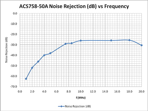
Table 4. Typical Capacitive Coupling of a 20 V Peak-to-Peak Signal on the Current Path

f (MHz) 1.0 2.0 3.0 4.0 5.0 7.5 8.5 10.0 15.0 18.0 20.0
VOUT(p-p) (mV) 15.0 50.0 100.0 200.0 250.0 700.0 750.0 1000.0 1020.0 1050.0 600.0
Noise Rejection (dB) -62.5 -52.0 -46.0 -40.0 -38.1 -29.1 -28.5 -26.0 -25.8 -25.6 -30.5


 stray magnetics
Figure 10. ACS758-50A Noise Rejection versus Frequency 


Yes, download from: CA/CB Package .stp model