Wide Input Voltage, 2.4 MHz, 3.5 A Asynchronous Buck Regulator

A8583

Product Image

Description

Top Features

Packaging

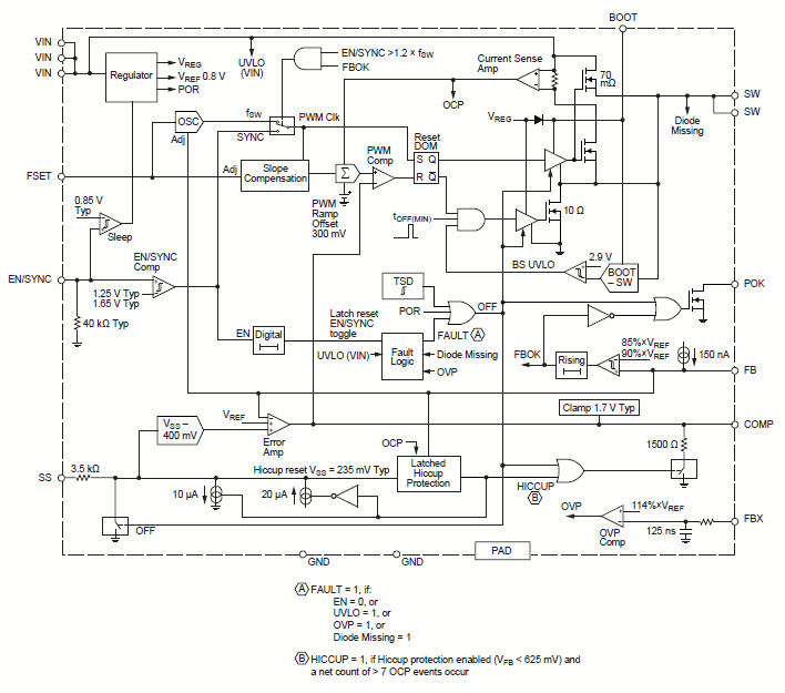
The A8583 is an adjustable frequency, high output current, PWM regulator that integrates a low resistance, high-side, N-channel MOSFET. The A8583 incorporates current-mode control to provide simple compensation, excellent loop stability, and fast transient response. The A8583 utilizes external compensation to accommodate a wide range of power components to optimize transient response without sacrificing stability.

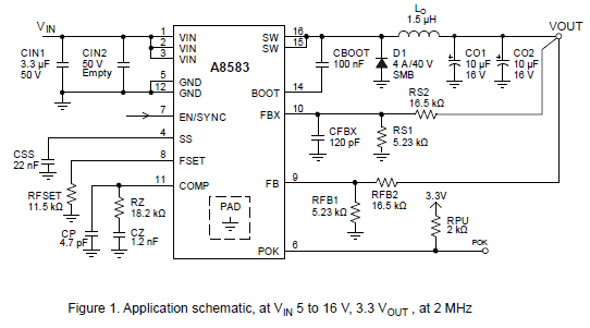
The A8583 regulates input voltages from 4.7 to 36 V, down to output voltages as low as 0.8 V, and is able to supply at least 3.5 A of load current. The A8583 features include an externally adjustable switching frequency, an externally set soft start time to minimize inrush currents, an EN/SYNC input to either enable VOUT and/or synchronize the PWM switching frequency, and a Power OK (POK) output to indicate when VOUT is within regulation. The A8583 only turns-on the lower FET to charge the boot capacitor when needed, not every PWM cycle. This improves light load efficiency and provides no-load currents as low as 3.5 mA at 2 MHz. The Sleep mode current of the A8583 control circuitry is less than 3 µA.

Protection features include VIN undervoltage lockout (UVLO), pulse-by-pulse overcurrent protection (OCP), hiccup mode shortcircuit protection (HIC), overvoltage protection (OVP), and thermal shutdown (TSD). In addition, the A8583 provides unique missing diode (D1) protection, open-circuit, adjacent pin short-circuit, and short-to-ground protection at every pin to satisfy the most demanding applications.

The A8583 device is available in a 16-pin TSSOP package with exposed pad for enhanced thermal dissipation. It is lead (Pb) free, with 100% matte tin leadframe plating.

  • Automotive AEC-Q100 qualified
  • Wide operating voltage range: 4.7 to 36 V
  • UVLO stop threshold is at 3.8 V (typ)
  • Supports 40 V input for surge and load dump testing
  • Capable of at least 3.5 A steady-state output current
  • Adjustable output voltage as low as 0.8 V
  • Internal 70 mΩ high-side switching MOSFET
  • Adjustable switching frequency, fSW: 0.25 to 2.4 MHz
  • Synchronization to external clock: 1.2 × fSW to 1.5 × fSW
  • Sleep mode supply current less then 3 µA
  • Soft start time externally set via the SS pin
  • Very low no-load current, typically 3.5 mA
  • Pre-bias startup compatible
  • Power OK (POK) output
  • Pulse-by-pulse current limiting (OCP)
  • Hiccup mode short-circuit protection (HIC)
  • Overtemperature protection (TSD)
  • Overvoltage protection (OVP)
  • Missing asynchronous diode (D1) protection
  • Open-circuit and adjacent pin short-circuit tolerant
  • Short-to-ground tolerant at every pin
  • Externally adjustable compensation
  • Stable with ceramic output capacitors
Typical Applications

The A8583 device is available in a 16-pin TSSOP package with exposed pad for enhanced thermal dissipation (suffix LP). It is lead (Pb) free, with 100% matte tin leadframe plating.

LP Package Documentation

Part Number Specifications and Availability