Automotive Grade, Fully Integrated, Hall Effect-Based Linear Current Sensor IC

ACS715

Product Image

Description

Top Features

Packaging

The Allegro ACS715 provides economical and precise solutions for DC current sensing in automotive systems. The device package allows for easy implementation by the customer. Typical applications include motor control, load detection and management, switched-mode power supplies, and overcurrent fault protection.

The device consists of a precise, low-offset, linear Hall sensor circuit with a copper conduction path located near the surface of the die. Applied current flowing through this copper conduction path generates a magnetic field which is sensed by the integrated Hall IC and converted into a proportional voltage. Device accuracy is optimized through the close proximity of the magnetic signal to the Hall transducer. A precise, proportional voltage is provided by the low-offset, chopper-stabilized BiCMOS Hall IC, which is programmed for accuracy after packaging.

The output of the device has a positive slope (>VIOUT(Q)) when an increasing current flows through the primary copper conduction path (from pins 1 and 2, to pins 3 and 4), which is the path used for current sensing. The internal resistance of this conductive path is 1.2 mΩ typical, providing low power loss. The thickness of the copper conductor allows survival of the device at up to 5× overcurrent conditions. The terminals of the conductive path are electrically isolated from the sensor IC leads (pins 5 through 8). This allows the ACS715 current sensor IC to be used in applications requiring electrical isolation without the use of opto-isolators or other costly isolation techniques.

The ACS715 is provided in a small, surface mount SOIC8 package. The leadframe is plated with 100% matte tin, which is compatible with standard lead (Pb) free printed circuit board assembly processes. Internally, the device is Pb-free, except for flip-chip high-temperature Pb-based solder balls, currently exempt from RoHS. The device is fully calibrated prior to shipment from the factory.

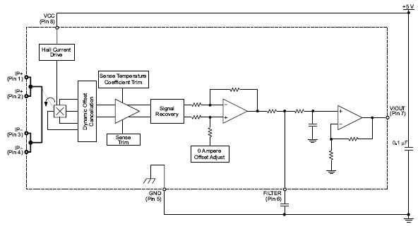
  • Low-noise analog signal path
  • Device bandwidth is set via the FILTER pin
  • 5 µs output rise time in response to step input current
  • 80 kHz bandwidth
  • Total output error 1.5% typical at TA = 25°C
  • Small footprint, low-profile SOIC8 package
  • 1.2 mΩ internal conductor resistance
  • 2.1 kVRMS minimum isolation voltage from pins 1-4 to pins 5-8
  • 5.0 V, single supply operation
  • 133 to 185 mV/A output sensitivity
  • Output voltage proportional to DC currents
  • Factory-trimmed for accuracy
  • Extremely stable output offset voltage
  • Nearly zero magnetic hysteresis
  • Ratiometric output from supply voltage
  • Operating temperature range, –40°C to 150°C

The ACS715 is provided in a small, surface mount SOIC8 package (suffix LC). The leadframe is plated with 100% matte tin, which is compatible with standard lead (Pb) free printed circuit board assembly processes. Internally, the device is Pb-free, except for flip-chip high-temperature Pb-based solder balls, currently exempt from RoHS.

LC Package Documentation

Part Number Specifications and Availability

Documentation and Resources

Documentation

Design Tools

Filter Document Type:
All Types
All Types Application Note Certificate
Documents Found: 32
Filter Document Type:
All Types
All Types Gerber File Simulation Tool Webpage
Documents Found: 32