Secrets of Measuring Currents Above 50 Amps
Introduction
It can be challenging to sense currents exceeding 50 A because the task often involves thermal management, must take place in a limited PCB area, and in some cases, requires a voltage isolation device. Two widely used methods for sensing high currents are a sense-resistor/op-amp approach, and Hall-based current sensing. It is useful to compare these two techniques. Recently developed Allegro MicroSystems integrated current sensors, ACS780LR and ACS770CB, will be used as examples.
It’s often best to measure current near the supply voltage of the load (the high-side) instead of near ground (the low-side). Measuring on the high-side brings immunity to ground bounces and allows for the detection of short circuits to ground. Depending on the supply voltage and the application, basic or reinforced isolation might be needed for sense-circuit connections. If a sense-resistor/op-amp are used to measure on the high-side, an op-amp with a high common-mode input range will be necessary, making the design more complex. To provide isolation, additional isolators (such as optocouplers) and isolated power supplies will be needed, increasing complexity and boosting costs.
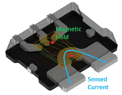
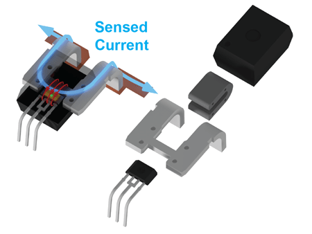
On the other hand, Hall-effect current sensor ICs, such as those provided by Allegro, eliminate the need for a sense resistor. The current flows directly into the integrated conductor, generating a magnetic field that will be measured.
ACS780LR 1
The ACS780 sits in a 6.4 × 6.4 mm surface mount LR package. Current flows into the integrated conductor and generates a magnetic field that on-die Hall elements then sense. Use of a flip-chip assembly technique brings the Hall elements close to the leadframe where the magnetic field is at its highest point. This packaging allows for superior signal-to-noise ratio.
The device uses two Hall elements to detect and reject any external stray magnetic field. The integrated conductor has a low 200 μΩ resistance to reduce power dissipation, allowing for more than 100 A of continuous current measurement with a 120 kHz bandwidth. Thermal performance depends highly on PCB design and layout.
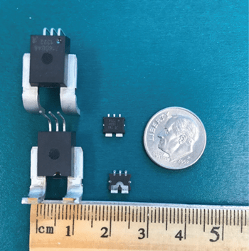
ACS770CB 2
The ACS770 sits in a 14 × 21.9 mm through-hole CB package. As current flows in its integrated conductor, an integrated low-hysteresis core concentrates the magnetic field which is then sensed by the Hall element with a typical accuracy of ±1% and 120 kHz bandwidth. The core also acts as a magnetic shield, rejecting external stray fields.
The integrated conductor has 100 μΩ resistance, providing ultralow power loss. The ACS770 can measure 200 A continuously at an ambient temperature of 85°C and can be factory programmed to measure inrush currents up to 400 A.
Thermal Performance
To determine the appropriate sensor for an application, it’s important to understand the thermal performance under high-level transient currents and constant DC/RMS currents. For the examples that follow, all measurements took place at 25°C ambient and could be used to derate the sensors at different operating temperatures.
High-Current Pulse Testing
LR Package
High-current pulse testing of the LR package took place using the Allegro ACS780 evaluation board. This is an eight-layer board with two-ounce (70 μm) copper and an FR4 substrate. Thirty-six thermal vias of 0.2 mm diameter were placed next to each of the solder pads of the integrated current conductor.
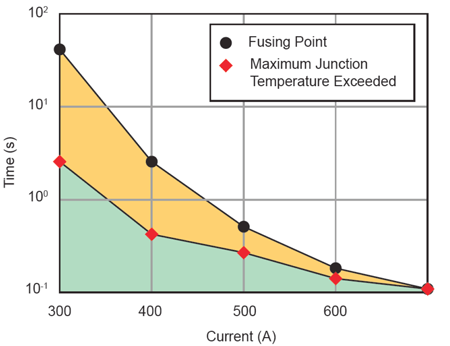
The package then experienced a current pulse of a set magnitude and the time was measured for two conditions: the time for the die temperature to exceed the maximum junction temperature of 165°C, and the time to fuse the current conductor open.
CB Package
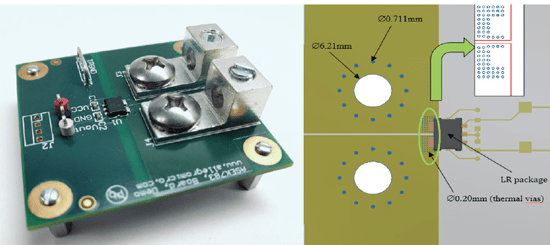
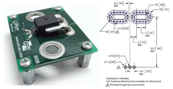
All testing of the CB package took place using the Allegro ACS770 evaluation board. This is a two-layer board with four ounce (140 μm) copper and an FR4 substrate. Sixteen thermal vias of 0.5 mm diameter were placed next to each of the solder pads of the integrated current conductor (Figure 6).
When subjected to high-current pulse testing, the CB package did not fuse at 1.2 kA—the maximum current capability of the lab equipment performing this measurement. The nearby table shows the maximum current pulse duration and duty cycle that could be applied to remain within the safe operating zone where the die temperature of 165°C is not exceeded.
Table 1: CB Package Overtemperature Time as Function of Applied DC Current
| Ambient Temperature (°C) |
Maximum Current (A) |
| Current is on for 10 s and off for 90 s, 100 pulses applied | |
| 25 | 350 |
| 85 | 350 |
| 150 | 260 |
| Current is on for 3 s and off for 97 s, 100 pulses applied | |
| 25 | 450 |
| 85 | 425 |
| 150 | 375 |
| Current is on for 1 s and off for 99 s, 100 pulses applied | |
| 25 | 1200 |
| 85 | 900 |
| 150 | 600 |
DC Current Capability
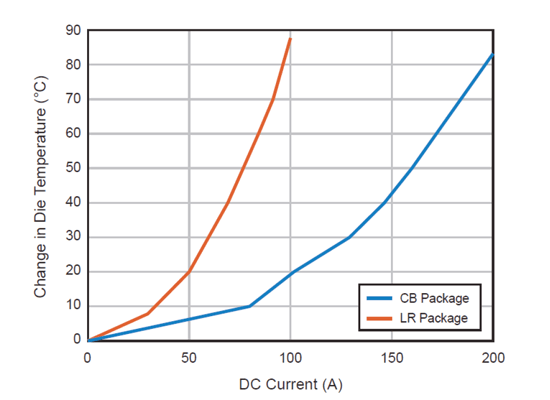
Figure 7 shows the die temperature rises as continuous DC current is injected through the sensors and temperature reaches steady state. As expected, the CB package shows a smaller temperature increase because of its lower conductor resistance of 100 μΩ compared to 200 μΩ for the LR package.
Layout Guidelines for Thermal Performance
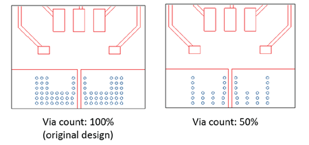
Increasing the LR Package Current Sensing Capability
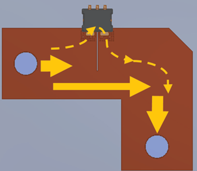
A simulation illustrates the thermal capability of this approach. Suppose a board is used with a current ratio of 6.7:1 (that is, current through trace: current through sensor) and the following specifications: six copper layers (top and bottom layer thickness of two-ounce (70 μm), inner layers of three-ounce (105 μm)), an FR4 substrate, 36 thermal vias of 0.2 mm diameter around each pad, and 5 mm diameter through-holes for current injection on the PCB. An aluminum heat spreader of 94 × 70 mm connects under the PCB.
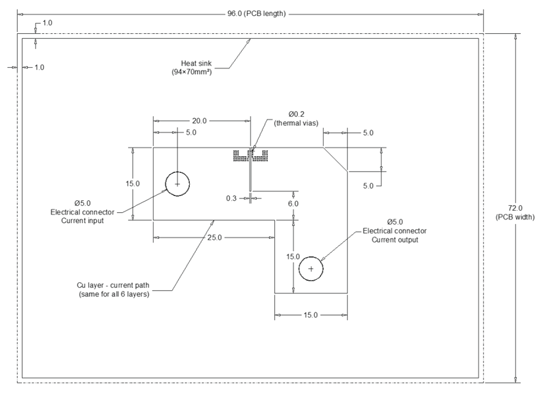
With 250 A injected in the PCB, a simulation assumed natural convection with an air enclosure volume of 300 × 300 × 300 mm with the enclosure wall set to 25°C. The highest observed temperature was 74°C on the top metal (~50°C rise relative to the ambient temperature), while the die temperature reached 71°C.
Isolation
Conclusion
Table 2: Comparing Sense-Resistor/Op-Amp and
Allegro Current Sensors when measuring >50 A
| Item | Sense-Resistor/Op-Amp | Allegro ACS780 | Allegro ACS770 |
| BOM | Increased BOM list including sense resistor |
Small surface-mount package with 150 A sensing range |
Through-hole package with 400 A sensing range |
| PCB Area | Larger BOM requires more PCB area |
6.4 mm × 6.4 mm | 14 mm × 21.9 mm |
| Power Dissipation | Higher resistance (2-4×) than ACS780, generates more heat on the PCB |
Integrated conductor resistance of 200 μΩ |
Integrated conductor resistance of 100 μΩ |
| Stray Magnetic Fields | Immune to stray magnetic fields | Differential sensing technique rejects stray fields |
Integrated concentrator core rejects stray fields |
| Isolation | Requires external isolators and more expensive isolated power supply |
For <100 V applications. Ideal for 48 V systems |
UL 60950-1 2nd edition passes 4.8 kV, providing a working voltage up to 990 Vpk. Ideal for line applications |
| Accuracy and Resolution | Accuracy will depend on resistance over temperature. Difficult to measure small currents with low sense resistor. Higher resistance provides good resolution but more power dissipation |
Typical accuracy of ±1%. Measures small currents and can resolve down to 60 mA with proper filtering |
|
| Noise | High inductance switching creates noisy events that require blanking and settling times |
Allegro IC filtering and integrated shield layer couple noise to GND and produces a cleaner output signal |
Footnotes:
- /en/Products/Current-Sensor-ICs/Fifty-To-Two-Hundred-Amp-Integrated-Conductor-Sensor-ICs/ACS780.aspx
- /en/Products/Current-Sensor-ICs/Fifty-To-Two-Hundred-Amp-Integrated-Conductor-Sensor-ICs/ACS770.aspx
Article published in Power Electronics Handbook, March 2017. Reprinted with permission.