Have Questions? Let us help!
We're passionate about innovation. Reach out and you'll hear back from an expert shortly.
One of our solution experts will be in touch with you shortly. Keep reading to learn more about our industry leading solutions.
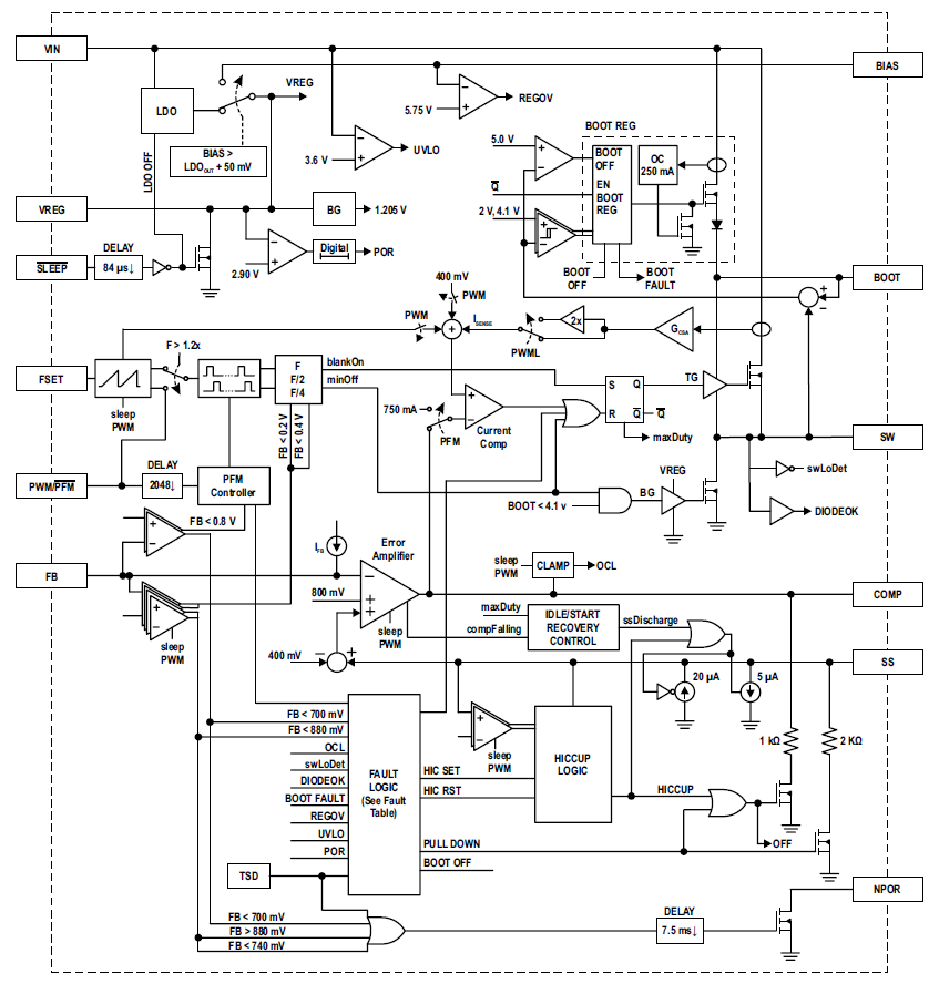
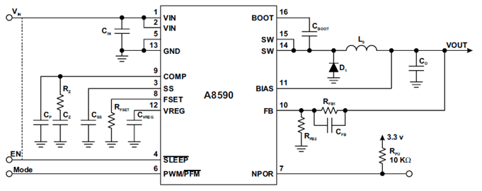
The A8590 offers robust and efficient power conversion for automotive applications, featuring low-Iq standby operation, a sleep mode, external synchronization, and enhanced idle/stop recovery for improved transient performance.