ACS709 Current Sensor IC Frequently-Asked Questions

The ACS709 current sensor family has the following advantages:
  • User-adjustable overcurrent fault level 
  • High speed overcurrent fault response (<2 µs) 
  • Wide bandwidth of 120 kHz 
  • Low noise, hence better current resolution 
  • Small footprint surface mount QSOP24 package  
  • High isolation voltage allows high working voltage 
  • Wide ambient temperature range for automotive applications  
The "optimized accuracy range," IPOA, is the current range around which the trimming of the ACS709 was done in the factory. The ACS709 will be almost just as accurate over the full linear sensing range, IR. 
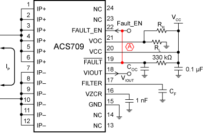
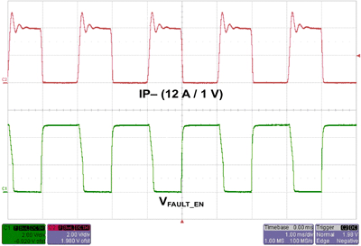
Yes. Just connect the FAULT_EN pin to the /FAULT output pin (shown as A in figure 1), to achieve automatic Fault reset. This configuration makes the circuit function as a current comparator. (See the oscilloscope plot in figure 2 for the input and output signal waveforms.) A capacitor, COC, is recommended to avoid any possible glitches at the /FAULT pin. It should be of appropriate value, usually greater than 1 nF, dependent on the noise environment and the Fault response time required.


Figure 1. Connection at A made to enable automatic reset of overcurrent fault.
 
 
 input-output waveforms
 Figure 2. Input (IP-) and output (FAULT_EN) signal waveforms of ACS709
configuration shown in figure 1 with COC = 100 nF.
Yes. The ACS709 family uses Hall-effect technology, which is capable of sensing electrical currents having both DC and AC components. As the datasheet states, the bandwidth of the ACS709 is 120 kHz typical. There may be phase lag and amplitude attenuation of the output for AC currents with frequency content greater than 120 kHz. For transient current signals, the response time is ≈ 4 µs.
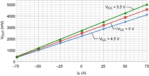
This feature is particularly valuable when using the ACS709 with an analog-to-digital converter. A-to-D converters typically derive their LSB from a reference voltage input. If the reference voltage varies, the LSB will vary proportionally. The ratiometric feature of the ACS709 means its gain and offsets are proportional to its supply voltage, VCC. If the reference voltage and the supply voltage for the ACS709 are derived from the same source, the ACS709 and the A-to-D converter will both track those variations, and such variations will not be a source of error in the analog-to-digital conversion of the ACS709 output. Figure 3 is a plot of primary current, IP, vs output voltage, VOUT, of the ACS709-35BB when varying VCC. The offset and sensitivity levels shift proportionally with VCC. For example, when VCC = 5.5 V, the 0 A output is 5.5 ⁄ 2 = 2.75 V nominal, and the sensitivity is 30.8 mV/A nominal.
 
Input versus Output
 
Figure 3. ACS709-35BB output voltage versus primary 
sensed current, at various supply voltage levels.
Allegro recommends the use of a 0.1 µF bypass capacitor between the VCC pin and the GND pin. The capacitor should be located as close as practicable to the ACS709 package body. Use of other external components depends on the application; please refer to Typical Application section of the datasheet.
No, the ACS709 sensitivity and 0-ampere quiescent voltage level are programmed at the factory.
The current resolution of the ACS709 family of sensor ICs is limited by the noise floor of the device output signal. For example, the ACS709-20BB version can resolve a change in current level of about 160 mA, at 25°C, at full bandwidth. The ACS709-35BB version can resolve approximately 210 mA. At these levels, the amount of magnetic field coupled into the linear Hall-effect IC is just above its noise floor. Resolution can be improved significantly by filtering the output of the ACS709 for applications requiring lower bandwidth. The noise level will, to the first order, scale proportionally with the square of the frequency. This means that the noise at lower bandwidths for the ACS709-20BB, can be approximated to be:
 
 Current resolution equation
 
Using the equation given above, table 1 gives resolution values for different filter capacitor values, CF, which forms a first order RC filter with the internal resistor RF(INT) (typical value 1.7 kΩ).
 

Table 1. ACS709-20BB Noise Level and Current Resolution
versus Filtering Capacitance and Resulting Bandwidth

CF
(nF)

BW
(kHz)

VRMS Noise
(µV)

VP-P Noise
(µV)

Current Resolution
(mA)

0

120

1500

9000

161

1

94

1327

7966

143

2.2

43

898 

5387 

96 

4.7

20

612

3674 

66 

10

9

411

2465 

44 

22

4

274

1643

30

 
Typical ESD tolerance is 6 kV Human Body Model, and 600 V Machine Model.
The capacitance between the ACS709 current carrying conductor and sensor ground is about 2 pF.
No, the ACS709 family is lead (Pb) free. All pins are plated with 100% matte tin, and there is no lead inside the package.
Yes, download from: ACS709 Gerber Files (ZIP).
Yes, a layout drawing PDF file can be downloaded from: ACS709 Layout Drawing (PDF).
Assumptions:
 
     A. The current carrying conductor is on the same plane as the Hall element, and
     B. The conductor has an infinite length
 
The result based on above assumptions will be the worst case result in terms of the influence of the stray field generated by the current carrying conductor on the Hall element.
 
The magnetic field generated in the direction perpendicular to the plane in which the conductor and the Hall element lie, at the distance l to the conductor will be:
 
Β = µ × I ⁄ (2π × L)   (tesla)
 
Where
     µ = µ0 = 4π × 10-7(H/m) = 400π(nH/m), assuming no core material around,
     I is in amperes, the current flowing in the conductor, and 
     L is in meters, the distance between the point under consideration and the conductor.
 
The analysis is based on the fact that the magnetic coupling coefficient of ACS709 family is typically 9.5 gauss per ampere (0.95 mT/A).
 
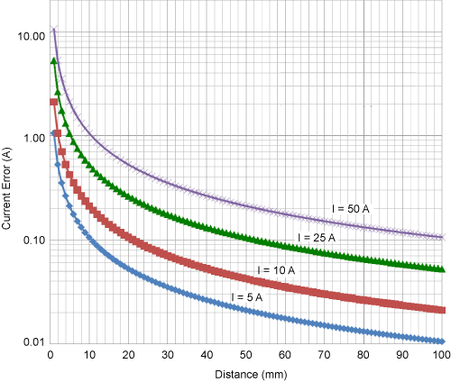
The graph in figure 4 shows absolute current error caused by a current carrying conductor which lies in the same plane as the Hall element, at various distances. The percentage error relative to full range and be calculated as:
 
Err = (absolute current error ⁄ IP) × 100    (%)
 
 Absolute Current Error
Figure 4. The absolute current error versus separation distance for various current values.
The ACS709 family has been certified by UL to the following standard: UL1577.

The mold compound is UL recognized to UL94V-0.
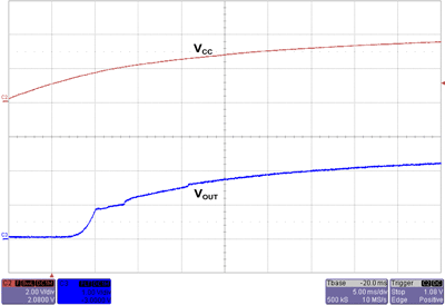
The typical output behavior of the ACS709-20BB during a slow ramp-up of VCC is shown for 0 A in figure 5 and for 12.5 A in figure 6.
 

Slow Vcc ramp at 0 A IP

Figure 5. VCC ramp-up with IP = 0 A.
 
Slow Vcc ramp at 12.5 A IP
Figure 6. VCC ramp-up with IP = 12.5 A.
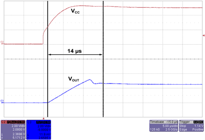
The typical time to valid output is given in table 3 and in figure 7 (IP = 0 A, VCC = 5 V) and figure 8 (IP = 12.5 A, VCC = 5 V). However, we recommend a 3X to 5X safety margin to account for power-on time variation over process and temperature ranges.
 

Table 3. ACS709-20BB Input Current versus Power-On Time

IP
(A)

tPO
(µs)

0

14

12.5

16


Startup at 0 A IP
Figure 7. Startup of ACS709-20BB with 0 A applied, then a VCC step from 0 to 5 V.
 
 
Startup at 12.5 A IP
Figure 8. Startup of ACS709-20BB with 12.5 A applied, then a VCC step from 0 to 5 V.
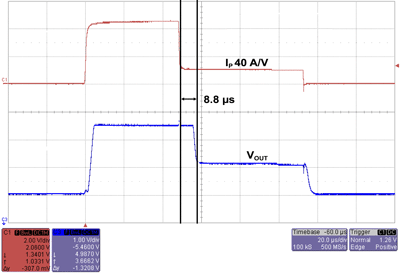
The ACS709-35B VIOUT response time from deep saturation was measured at less than 9 µs. Please see the oscilloscope plot in figure 9 for details.
 
VIOUT from saturation
Figure 9. Test conditions: for saturation, VCC = 5 V, TA = 25°C,
IP = 180 A; for linear VIOUT, Ip = 40 A.
 
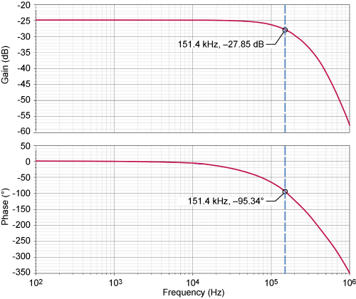
The graph in figure 10 shows the results of a high level frequency response simulation of the ACS709 current sensor IC circuit. The plot on the top is the amplitude response and the plot on the bottom is the phase response.
 
Frequency response
Figure 10. Frequency response of the ACS709.
The output of the sensor may oscillate.
The ACS709 may not produce an valid output, because the output driver will not be able to supply sufficient current.
The following overcurrent limit results are based on the Allegro ASEK709 evaluation board. The limits may be different on a different application board. For detailed information on the Allegro ASEK709 evaluation board, please see FAQ Can I get the Gerber files for your evaluation board?.
 
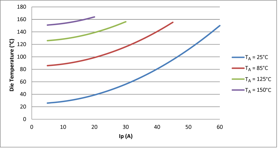
Table 4 presents results for continuous DC current, and table 5 presents results for pulsed current. Figure 11 shows the effects of various input current levels on die temperature.


Table 4. Continuous Current Overcurrent Limits
ASEK709 evaluation board, at various ambient temperatures

tA
(°C)

IP(OClim)
(A)

25

50

85

40 

125

25

150

20


Table 5. Pulsed Current Overcurrent Limits
ASEK709 evaluation board, at room temperature

IP
(A)

Duration
(ms)

Duty Cycle
(%)

Quantity of
Pulses Allowed

100

1000

NA

Single

100

300

30

20

150

200

NA

Single

150

100

10

20 

200

50

NA

Single

200

20

10

20


Die temperature
 
Figure 11. ACS709 die temperature (°C) versus continuous DC IP current (A)
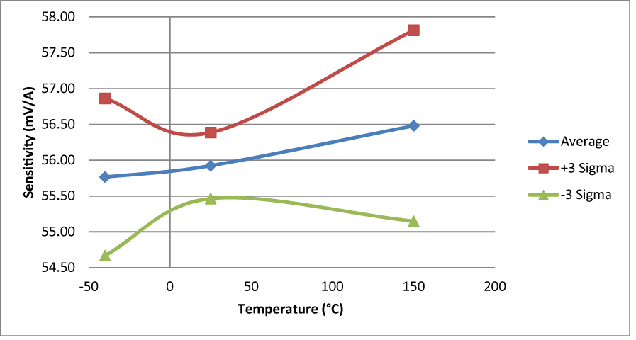
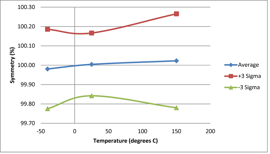
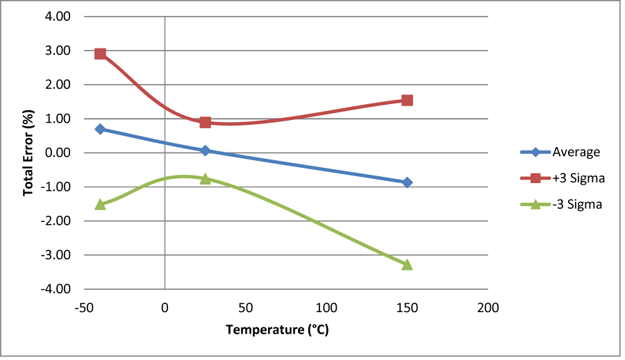
Please see the graphs in figure 12 for the distribution data from a group of ACS709-20BB devices characterized for (12A) sensitivity, (12B) non-linearity, (12C) symmetry, and (12D) total error.
 
 
Figure 12A. ACS709-20BB Sensitivity versus Ambient Temperature at IP = 37.5 A


Figure 12B. ACS709-20BB Nonlinearity versus Ambient Temperature at IP = 37.5 A


Figure 12C. ACS709-20BB Symmetry versus Ambient Temperature at IP = 37.5 A


Figure 12D. ACS709-20BB Total Error versus Ambient Temperature at IP = 37.5 A
 
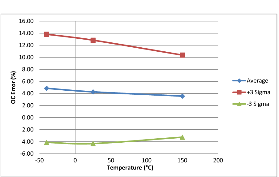
The graph in figure 13 shows the distribution of the overcurrent fault level error over a range of operating ambient temperatures. The data is taken from a limited number of devices and is for reference only.


Figure 13. ACS709-20BB Overcurrent Fault Error versus Ambient Temperature
 
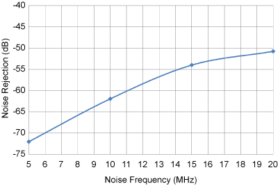
The leadframe noise rejection test is conducted by injecting a high-frequency sinusoidal frequency onto the high-current leads. The signal coupling onto the output of the Hall-effect device is then measured. The ACS709 family devices exhibit a high level of leadframe noise rejection as table 6 reveals. In addition, figure 14 indicates performance as a function of frequency.
 

Table 6. Typical Capacitive Coupling of 
20 Vp-p Signal on the Sensed Current Path

Frequency
(MHz)

VOUT
(mVp-p)

Noise Rejection
(dB)

5

5

−72

10

16

−62

15

40

−54

20

58

−51


Capacitive coupling
Figure 14. ACS709 noise rejection versus noise frequency