Method for Converting a PWM Output to an Analog Output When Using Hall Effect Sensor ICs
A current sensor with PWM output is a very useful type of device. Traditionally, the device can serve in a digital application where the host microcontroller can determine the ratio of the on-time to the off-time of the sensor output signal. Another useful way to use a PWM sensor is to convert the PWM output signal into an analog output signal. The goal of this article is to briefly introduce a simple way to convert the PWM signal into an analog signal, along with some examples and important design constraints.
How PWM Output Sensors Work
Before getting too deeply into designing a filter, the first step is to quickly review what the output signal of a PWM sensor looks like. The PWM waveform is basically a square wave, with a frequency we will define as fPWM , and an amplitude that is 0 V for logic low, and VCC for logic high. From here forward, we will refer to the amplitude as VPWM . The ratio of the signal high time, tON , to the period (TPWM = 1 / fPWM ) is the duty cycle, D. These relationships are diagrammed in figure 1.
The duty cycle for a PWM output Hall IC is proportional to the sensed magnetic field. As the input field increases in strength, so does D (figure 2). Conversely, as the input field decreases, so does D (figure 3).
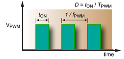
Figure 1. Basic PWM Definitions
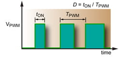
Figure 2. PWM for an increasing field
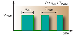
Figure 3. PWM for a decreasing field
How Analog Output Sensors Work
Now that we reviewed how a PWM output works for a Hall-effect IC, it is time to briefly discuss how an analog output works for a sensor. The premise is nearly identical as that for the Hall IC with a PWM output. Except, instead of a constant switching of the output to generate a signal, the output asserts an analog voltage that is proportional to the sensed magnetic field. For example, when the PWM duty cycle would increase due to a rising input field, the analog output would simply rise to a higher DC voltage, and vice versa for a decreasing field.
Passive Filters
Now we come to the interesting part of the process, where we create an analog DC voltage from the PWM output signal. The simplest method for this is with a passive low pass filter. For the purposes of this guide, and for simplicity, the focus will be on passive, first and second order, low pass filters. Passive filters can be realized very simply with resistors and capacitors. The concepts presented here can be applied to more advanced filters.
For the purposes of this document, we will be focusing on analyzing and designing circuits that use passive low pass filters with attenuation roll-off factors of –20 dB / decade for first order filters and –40 dB / decade for second order filters. In some cases, a first order filter will work fine. However, some applications may require a faster response time. In these cases, a second order filter may be necessary. It is up to the end user to evaluate the tradeoff between cost of the filter and the filter performance. The order of the filter can be increased by simply cascading more and more stages. For each additional order of the filter, the roll-off rate becomes steeper, by an additional –20 dB / decade.
There are a couple of ways to compute the filter response to an input signal: time analysis and frequency analysis. I prefer back-of-an-envelope frequency analysis, and will be focusing on using frequency analysis techniques to design first and second order low pass filters. In general, most folks without an electronics background understand frequency methods better than time domain methods when designing simple filters.
Back of the Envelope Filter Design
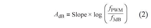
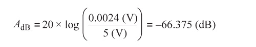
While there are many detailed ways to compute filter requirements and filter output ripple voltage, I prefer to keep things simple in such a way that I can draw up and design a simple filter on the back of a small envelope and make calculations with a cheap scientific calculator (or smart phone app). The first term you have to define is how much ripple voltage, VRIPPLE , is acceptable in the analog output. The second necessary term is the PWM frequency, fPWM , of the sensor. Once the acceptable VRIPPLE and fPWM are defined, the required attenuation can be computed. Because we are working in the frequency domain and using known filters, it is most useful to compute this attenuation factor in dB:
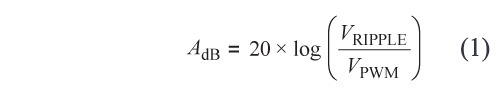
where AdB is attenuation, and must be a negative number! Remember that VPWM is simply the output voltage swing of the PWM sensor.
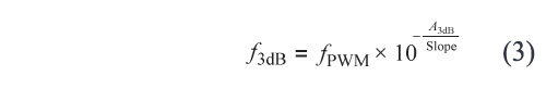
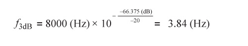
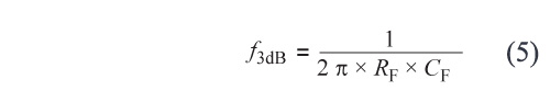
Once the attenuation factor is known we can apply our knowledge, that the slope of a first order low pass filter is –20 dB / decade and the slope of a second order low pass filter is –40 dB / decade, to determine the required 3-dB frequency (f3dB ) for the filter:
What this equation is telling us is that the attenuation, AdB , is equal to the slope (dB / decade) of the low pass filter, times how many decades are between the 3-dB frequency (f3dB) and the PWM frequency (fPWM). Since we already know AdB , we will solve the following equation for what we want to know, f3dB :
Now we have everything we need to design a passive low pass filter. While this may seem a little complicated, trust me, it is easier than solving second order time domain equations.
Another interesting exercise is to set equation 1 equal to equation 2 and solve for VRIPPLE . This will give us an equation that expresses voltage ripple as a function of f3dB :
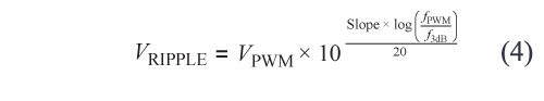
While this equation is a little more complicated than the previous three equations, it has pretty simple mathematics that allow us to plot ripple voltage versus 3-dB frequency for determining known slope, PWM voltage, and PWM frequency.
Figure 4 plots approximate VRIPPLE versus f3dB for first and second order filter slopes, given fPWM = 8 kHz and VPWM = 5 V. This chart can be used as a guide for designing a filter. Simply select the required amount of ripple on the vertical axis, and then find where the two lines intersect this horizontal line. These intersections are where the filters will achieve the target requirements.
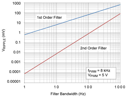
Figure 4. Ripple Voltage versus 3-dB frequency; use for estimating first and second order filters
It should be noted that these calculations will have some error in them when compared to actual measured ripple voltage. One source of error is due to the fact that the corner frequency of the filter is not a perfect corner. It is in fact rounded. This means that the attenuation of the filter near the corner does not follow our 20 dB/decade approximation perfectly. The story is the same for higher order filters as well.
Another source results from computing the amplitude of our ripple by focusing on the fundamental frequency of the PWM. In reality, the PWM will have higher frequency content because it is a square wave. More specifically, we are omitting the odd harmonics of the fundamental (3 × fPWM , 5 × fPWM , 7 × fPWM , …). Fortunately for us, the attenuation of those higher frequencies from our filter is even greater than for the fundamental. For the most part, they can be ignored for the first iteration of the filter design. As for our back-of-the-envelope calculation, we get very close to the actual value without unnecessarily complicated computations. Oftentimes the first order filter pole must be adjusted downward a little bit to achieve the target ripple, due to the shallower roll-off of –20 dB / decade. The simulations below will illustrate this point.
Example:
Let us say that we have a sensor with an fPWM of 8 kHz, a VPWM of 5 V, and we are targeting LSB / 2 of ripple for our 10-bit A‑to‑D converter. For this case, LSB / 2 corresponds to about 2.4 mV of voltage ripple. So, the first thing we need to do is calculate the attenuation factor we need. Using equation 1:
Now that we know the attenuation factor, the next step is to compute the bandwidth of the filter we need to design, using equation 3. We will do this twice, once for a first order filter:
and again for a second order filter:
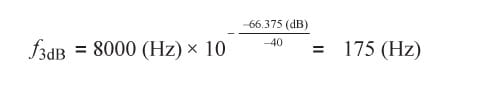
So if we use a first order low pass filter, we would need to design a filter with an f3dB of 3.84 Hz. This may not be attractive depending on the rest of the system requirements. A second order filter would require an f3dB of 175 Hz. This may be a more attractive option for some applications that require faster transient response.
Building the Filter
Constructing a basic passive low pass filter is quite simple. A first order filter uses one capacitor and one resistor, and a second order filter uses two resistors and two capacitors. The extra resistor, RL , in the schematics (figures 5 and 6) is there to represent a typical input resistance of the measurement system.
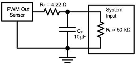
Figure 5. First-Order Low Pass Filter for 3.77 Hz
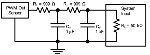
Figure 6. Second-Order Low Pass Filter for 175 Hz
We will build the first order filter first. Building a first order filter is as simple as choosing a starting capacitor value, and then computing the resistor value.
Given:
and
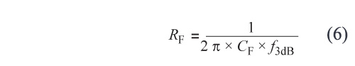
For the first order filter (f3dB = 3.84 Hz), we can chose a capacitor, CF , value of 10 μF and use equation 6 to compute that the filter resistor, RF , value:
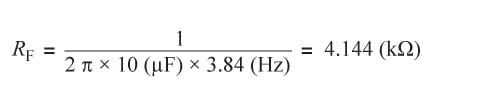
RF should be rounded up to the closest 1% resistor value of 4.22 kΩ, and the corresponding f3dB value would be 3.77 Hz.
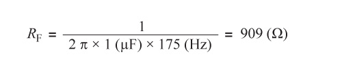
The implementation for a second order passive low pass filter is simply cascading two first order filters in series. In this example, we will create two first order filters, each with an f3dB of 175 Hz as calculated above using equation 3. For this example, we chose 1 μF for CF and computed RF to be 909 Ω (standard 1% value) by substituting into equation 6:
Simulated Results
The following several figures illustrate simulation results of the two filters designed in this article. The PWM output was configured such that fPWM = 8 kHz, D = 50%, and VPWM = 5 V, as shown in figure 7. This figure represents the unfiltered input signal. Remember that we will be applying a much slower filter to this waveform, so many of the following graphs are at a different time scale.
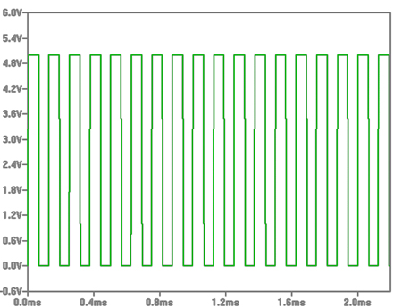
Figure 7. Input PWM signal (fPWM = 8 kHz)
Figure 8 illustrates the output transfer function of the waveforms in figure 4 for both the first order (green trace) and the second order (blue trace) filters. It is obvious to see that the lower frequency f3dB of the first order filter causes a much slower response. It is also apparent that the series resistance of the filter does impact the voltage of the output signal, as there is indeed a resistor divider that reduces the voltage at the system input (4.22 kΩ for the filter and 50 kΩ for the approximated input resistance of the system). Overall, the response of the curves is what was expected from our calculations.
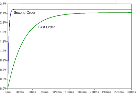
Figure 8. Output Response of first and second order filters
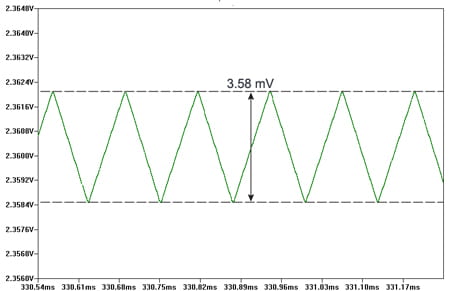
Figure 9. Detail of output ripple for first order filter simulation, ripple = 3.58 mV
Next we need to have a closer look at the ripple voltage of the settled output waveform. Figure 9 shows the detailed view of the ripple of the first order filter output. It shows that the final ripple value is 3.58 mV for our f3dB of 3.77 Hz. It is a little bit higher than we were targeting, but as stated before, it was expected that we may be off by a little bit, based on our assumptions. However, our filter is definitely performing in that region and could be slightly adjusted. Increasing RF or CF slightly will reduce the ripple. Increasing RF or CF will also lower f3dB. Simulation experiments will show that moving f3dB down to about 2.57 Hz by changing RF to 6.19 kΩ will bring the ripple into specification.
Figure 10 shows a zoomed in version of the output ripple for the second order low pass filter. Here we can see that we were even closer with our original design estimate. This filter achieved a ripple voltage of 2.86 mV. Not bad since we were shooting for 2.4 mV. Once again, this ripple value can be reduced by modifying the filter slightly and lowering f3dB in a similar manner as the first order example.
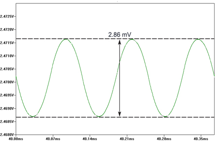
Figure 10. Detail of output ripple for second order filter simulation, ripple = 2.86 mV
Lab Data
A filter design and simulation exercise would not be complete until the filter has been constructed and tested in the lab. The last two figures (11 and 12) are oscilloscope images of the output ripple for each of the two filters. The filters were constructed with the original design components earlier in a solderless breadboard. The input PWM and the output analog voltage were measured using an oscilloscope. The two figures illustrate that our filters performed very close to the original design targets.
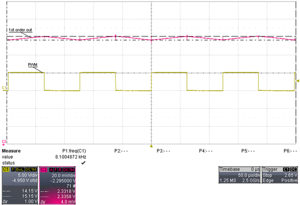
Figure 11. First-order filter output lab results, VRIPPLE = 4.0 mV
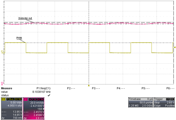
Figure 12. Second-order filter output lab results, VRIPPLE = 2.8 mV
Conclusion
This article briefly summarized a simple method for converting the output of a PWM sensor to an analog voltage. The methods shown use a fairly straightforward method for designing a filter as well as documenting the caveat for using the simple method. The primary goal of showing how to realize a passive low pass filter was illustrated with a first order filter, and a second order filter. The reader can extend the order of the filter in order to increase the response time of the signal while maintaining acceptable ripple. Note: A third order filter rolls off at –60 dB / decade, but requires 2 more passives.
The worked examples show that unless a very slow response time is acceptable, most typical applications will want to pursue a second order (or higher) low pass filter in order to keep the filter response fast enough, and to maintain the use of small components. Increasing the order of the filter increased the number of passive components required to realize the filter. In this case, we went from two total passives to realize a first order filter, to four total passives to realize the second order filter.
Although every system is different, the methods in this document can be used for many different systems. Some PWM signals have a different fPWM . By using the equations documented above, a filter can be designed around a different system. Slower fPWM will require lower f3dB , while faster fPWM can get away with higher f3dB . In closing, with a little bit of creative filter design, an off-the-shelf PWM output sensor can be designed into a system that requires an analog voltage.
Copyright ©2013, Allegro MicroSystems, LLC
The information contained in this document does not constitute any representation, warranty, assurance, guaranty, or inducement by Allegro to the customer with respect to the subject matter of this document. The information being provided does not guarantee that a process based on this information will be reliable, or that Allegro has explored all of the possible failure modes. It is the customer’s responsibility to do sufficient qualification testing of the final product to insure that it is reliable and meets all design requirements.
Ref: 296094-AN