Wettable Flank Plated PQFN
By Bradley Smith,
Allegro MicroSystems, LLC
Background
Plastic Quad Flat Pack No-Lead (PQFN) or Quad Flat Pack No-Lead Exposed Pad (QFN-EP) packages [a.k.a. QFN) have no easily solderable, visually exposed terminations, because the package designs have terminations on the underside of the package for solder joints. The package edge has exposed copper of the termination after singulation and does not easily solder wet due to copper oxidation. Therefore, visual determination that the package has soldered effectively cannot be made optically or by x-ray. Electrical test is the only way to determine electrical connectivity of the soldered terminations. There are some applications where full electrical test of all terminations is difficult or incomplete. Thus, in high reliability applications, it may be desired to visually check for termination solder joint integrity. It is for these purposes that wettable flank, tin plated terminations of QFNs have been developed as a visual aid to the determination of board solder operation effectiveness.
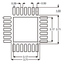
Figure 1: PCB Land Layout for 5 mm x 5 mm 28-Lead PQFN
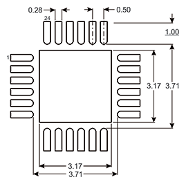
Figure 2: PCB Land Layout for 4 mm x 4 mm 24-Lead PQFN
Wettable Flank Plating
In a typical QFN assembly operation, the package body of an individual device is singulated and separated from a “brick” by a sawing operation, which leaves an exposed copper sidewall for each termination. Since this exposed copper does not have any plating, the copper oxidizes. When the device is soldered onto a circuit board, these sidewall areas do not solder consistently. Wettable flank plating is an additional process step which puts a 100% tin plate, with the normal tin plating thickness, on the package underside terminals and an exposed flank. The wettable flank plating is protective of the copper and allows soldering to occur on this external flank area such that optical inspection can be made verifying a good solder fillet joint, and thus a good electrical connection.
Board Solder
A standard QFN board layout is used for sidewall plated parts with the addition of extended terminal lands 40 mil (1.00 mm) in length (see Figures 1, 2) and of 31.5 mil (0.80 mm) (refer to Figures 3 and 4). This allows additional solder paste to flow to the terminal wettable flank and form a solder fillet there which can be visually identified. Standard rosin or water-based no-clean flux lead-free (SAC305 or equivalent) solder pastes can be used with a nominal screen thickness of 0.127 mm (5 mil). Stencil land length should be extended an additional 0.20 mm. Therefore, 1.0 mm terminal lands should be extended to 1.2 mm, and 0.8 mm terminal lands should be extended to 1.0 mm. Reflow conditions should have a peak temperature no lower than 230ºC, typically 245ºC, and no higher than 260ºC, and use a nitrogen blanket or air. If nitrogen reflow is available, better wetting and consistency may occur, regardless of temperature, flux system, or alloy used. Typical package sizes are 5 x 5 mm (28L), 4 x 4 mm (24L and 20L), and 3 x 3 mm (10 leads--5 on two sides). Note that the above terminal land lengths are recommended, but customers may wish to use 20% shorter lengths to accommodate a particular solder paste/flux system and optical inspection tool preference.
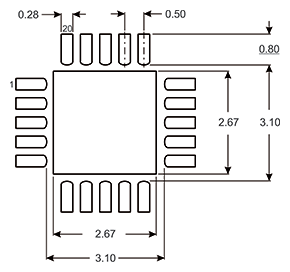
Figure 3: PCB Land Layout for 4 mm x 4 mm 20-Lead PQFN
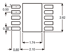
Figure 4: PCB Land Layout for 3 mm x 3 mm 10-Lead PQFN
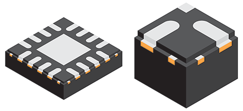
Figure 5: Sensor IC Prepared for Wettable Flank
The wettable flank process makes a partial cut into the terminal edge to expose a side flank. In the next step of tin plating, the flank is plated
with the full tin thickness. Image to the right shows the detail of the exposed flank, which is tin plated.
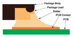
Figure 6: Illustrated Cross Section Showing a Solid Solder Fillet, that is Optically Inspectable, has Formed with the PCB Board
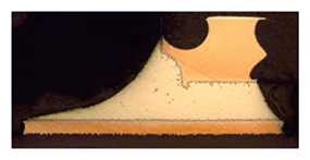
Figure 7: Photographic Actual Cross Section Showing a Solid Solder Fillet, that is Optically Inspectable, has Formed with the PCB Board
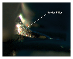
Figure 8: Ideal Solder Fillet (230ºC, 40 mil pad length, 8-hr
steam preconditioning), Side View, Optically Inspectable
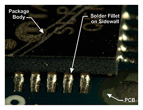
Figure 9: Visually Inspectable Solder Fillet (245ºC, 40 mil pad length, 8-hr steam preconditioning)
Visual Examination of Solder Wetting
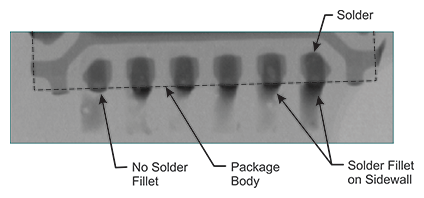
Figure 10: X-ray of Solder Fillets at Sidewall Terminations
Observation looking directly down on the device (90º) shows wetting of the lands and the wettable flank. In addition, x-ray can show (with an unobstructed board) that sidewall fillets have formed. A black band at the package edge shows the thick solder fillet (see Figure 10).
Refer to IPC-A-610 Spec Acceptability of Electronic Assemblies section 8.2.13 Plastic Quad Flat Pack-No Leads (PQFN) and note the maximum side overhang is 25% of termination width and the minimum end joint width is 75% of termination width. The minimum toe (end) fillet height up the termination sidewall is not specified by Allegro but is generally observed at more than 50% of the wettable flank height using nitrogen reflow. Refer to Application Information “Soldering Methods for Allegro Products (SMD and Through-Hole)” at Allegromicro.com; Design Center; Packaging, for information on reflow profiles and considerations.
Allegro warrantees that the device will be reliable and electrically connected by the solder terminations under the package body regardless of the degree of sidewall soldering.
Copyright ©2017, Allegro MicroSystems, LLC
The information contained in this document does not constitute any representation, warranty, assurance, guaranty, or inducement by Allegro to the customer with respect to the subject matter of this document. The information being provided does not guarantee that a process based on this information will be reliable, or that Allegro has explored all of the possible failure modes. It is the customer’s responsibility to do sufficient qualification testing of the final product to insure that it is reliable and meets all design requirements.