Overcoming Size Challenges in PCB Design with Magnetic Current Sensors

Article 1 of Next-Generation Current Measurement Series: Magnetic current sensors provide a compact and efficient alternative to traditional current measurement techniques that significantly reduce the size of components on PCBs, crucial for space-constrained electronic designs.
As the demand for smaller electronic devices increases, engineers face significant challenges in integrating all necessary components within constrained PCB areas. One critical aspect of electronic design is current measurement, which is vital for monitoring and controlling energy usage, ensuring safety and enhancing the overall performance of electronic systems. However, traditional current sensing methods, especially those involving shunt resistors, present several challenges. These methods often require additional amplifiers and filters, which not only consume valuable PCB space but also elevate production costs. Magnetic current sensors emerge as a viable alternative, offering the potential to significantly reduce PCB footprint by integrating multiple discrete components into a single integrated circuit.
In our Next-Generation Current Measurement series, we've previously explored various challenges associated with traditional current sensing methods. This article focuses specifically on addressing the challenge of size constraints within PCB design and highlights the advantages of magnetic current sensors in modern electronics.
Current Sensing and Space Constraints
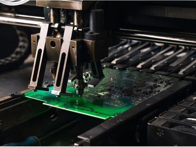
In traditional PCB design, managing current sensing typically involves the use of shunt resistors along with ancillary components such as operational amplifiers, filtering components and gain-setting resistors. These components consume a significant area of the PCB and add complexity to the layout, which makes it challenging to achieve the compactness required by electronic devices.
Using a number of components necessitates additional design considerations such as thermal management and precise routing for effective electrical isolation and accurate signal measurement, for instance, ensuring Kelvin connections to the shunt resistor. This complexity can increase the overall PCB size, which in turn raises material costs and necessitates larger enclosures, thereby driving up manufacturing expenses.
.jpg?sc_lang=en&hash=5687F1EA088021DD67CB11F5AF3026C8)
Magnetic current sensors offer a streamlined solution to this problem by incorporating all necessary functionalities into a single small package.
.jpg?sc_lang=en&hash=870F295CD5E4802D1B962242B57A4B00)
These integrated magnetic current sensors eliminate the need for external components, which are often larger than the magnetic sensor’s package itself, thereby simplifying the PCB layout and significantly reducing the footprint required for current sensing. This integration enables more efficient use of space and resources in designing advanced electronic systems.
Minimizing PCB Footprint with Magnetic Current Sensing
Magnetic current sensors represent a breakthrough in current sensing technology by integrating the functions of shunt resistors, shunt amplifiers, and additional filtering components into a single compact integrated circuit (IC). This integration streamlines the design process and drastically reduces the physical footprint on the PCB.
Comparison with Traditional Shunt Resistors
A typical 1 mΩ shunt resistor in a 2512 package (6.3 x 3.2 mm) occupies a substantial PCB area. In contrast, Allegro’s ACS71240, with a 0.6 mΩ resistance in a 3 x 3 mm QFN package, is 56% smaller, occupying just 9 mm².
A complete shunt-resistor-based current measurement circuit, with a resistance of 0.5 mΩ, having similar functionality, consumes 120 mm², making it nearly 13.3 times larger than the ACS71240 solution.
.jpg?sc_lang=en&hash=47D7C9653CFCB4BB00A5D25ECD19E108)
For high-current applications, where a 100 µΩ shunt resistor might require an even larger footprint (around 10 x 5.2 mm), Allegro’s ACS37220 in a 4x4 mm QFN package reduces size by 69% by integrating up to 9 distinct components on the board, resulting in substantial space savings.
.jpg?sc_lang=en&hash=4F6FF1338C503FBE518A50CFB1800A3D)
These examples highlight how magnetic current sensors can drastically decrease the PCB area required for current sensing.
Key Benefits of Magnetic Current Sensors
The integration of magnetic current sensors into PCB designs provides several distinct advantages specifically related to addressing size constraints, a critical issue highlighted in our previous discussion. These benefits offer compelling solutions over traditional shunt-based approaches where space is limited.
Reduced PCB Area
Integration Efficiency: By combining the functionalities of current sensing, amplification and filtering into a single component, magnetic current sensors significantly decrease the PCB footprint. This is beneficial in applications where space is scarce, such as in automotive systems.
Simplified Layout: The reduced number of components simplifies the PCB layout to minimize the need for additional wiring and routing, which can complicate the assembly process and increase the risk of errors.
Cost Efficiency
Lower Material Costs: Smaller PCBs require less material, which directly reduces the cost of the product of which they are a part. Additionally, smaller boards can fit into smaller enclosures, which are often less expensive and reduce the overall material expenditure for the product.
Reduced Assembly Costs: With fewer components to place and solder, assembly time and costs are reduced. This streamlined assembly process can also decrease the likelihood of manufacturing defects to further reduce costs associated with quality control and rework.
Design Flexibility
Innovative Product Design: The space savings provided by magnetic current sensors enable designers to either reduce the size of the existing products or use the available space for additional functionality, which potentially differentiates their products in competitive markets.
Enhanced Performance and Reliability: With fewer components involved, the overall reliability of the PCB can increase as there are fewer potential points of failure. Additionally, the integrated design of magnetic sensors often comes with improved performance characteristics, such as enhanced noise immunity and better thermal management.
These benefits make magnetic current sensors an attractive option for a wide range of applications, particularly those where innovation and cost-effectiveness are crucial.
Case Study: Real-World Application and Benefits
A compelling example of the benefits offered by magnetic current sensors can be seen in the experience of a global industrial robot manufacturer. This company faced significant challenges in incorporating traditional shunt resistors into their designs due to the large size and complex integration requirements. The small form factor required for their advanced robotic systems made traditional current sensing methods impractical.
Challenge Faced
The manufacturer needed a current sensing solution that could fit within the stringent size constraints of their robotic systems without compromising on performance. Traditional shunt resistors, along with their auxiliary components, were simply too bulky and would have necessitated design compromises that could affect the overall functionality of the robots.
Solution Delivered
The company opted to integrate Allegro’s ACS71240 magnetic current sensors into their designs. These sensors offered a much smaller footprint compared to the shunt resistors previously considered. The ACS71240 sensors, housed in compact 3x3 mm QFN packages, provided the necessary current sensing capabilities while meeting the size requirements imposed by the compact robotic designs.
Outcome Achieved
The transition to magnetic current sensors enabled the manufacturer to achieve several key improvements:
- Space Efficiency: The smaller sensors allowed for a more compact overall design, crucial for the intricate internal layouts of their robots.
- Enhanced Performance: With integrated signal conditioning and improved accuracy over traditional methods, the sensors delivered more reliable and precise current measurements.
- Cost Reduction: By reducing the PCB size and simplifying the assembly process, the manufacturer could lower both production costs and time-to-market for their robotic systems.
This case study is proof of the drastic impact that magnetic current sensors can have on product design and manufacturing.
Overcoming Size Challenges in PCB Design with Magnetic Current Sensors by Allegro MicroSystems
Innovations in current sensing technology are crucial for enhancing the efficiency and functionality of PCB designs in constrained spaces. Allegro MicroSystems offers a range of integrated solutions that cater to different needs, from high-current applications to compact, high-voltage environments.
Allegro ACS37041: This sensor, enclosed in a compact SOT23-W package, supports bidirectional current measurement up to 30 A and operates up to 100 V(RMS). Its low resistance of 1.6 mΩ and error below ±5% across the temperature range make it ideal for various applications where board space is limited but precise current measurement is crucial.
.jpg?sc_lang=en&hash=FDF6DD69F7BEC0EB87286DB0FF031F3C)
Allegro ACS37220: Designed for high-current applications, this sensor comes in a 4 x 4 mm QFN package, can handle up to ±200 A, and operates under 100 V(RMS). It features an ultra-low 100 μΩ resistance conductor and is AEC-Q100 certified, optimal for automotive and data center applications where high reliability and performance are required under stringent conditions.
.jpg?sc_lang=en&hash=36D603277D9225ECD0BBCF60F94AA195)
Allegro ACS71240: Available in 3mm x 3mm QFN and SOIC8 packages, this sensor measures currents up to 60 A (QFN) and 55 A (SOIC8), and withstands voltages up to 420 V(Peak) and 297 V(RMS). Key features include immunity to stray magnetic fields, fast overcurrent fault output and AEC-Q100 qualification, which makes it ideal for applications that require compact design in high-voltage environments.
.jpg?sc_lang=en&hash=4BC6600897BB6ED528D051BF2ADDDB8A)
Together, these sensors demonstrate Allegro’s commitment to providing scalable solutions for PCB designs that demand high performance in space-constrained environments. Each sensor is tailored to meet specific application needs to ensure that design engineers have the right tools to address modern electronic challenges efficiently.
Conclusion
As electronic devices continue to shrink, the need for compact and efficient design solutions becomes increasingly critical. Magnetic current sensors address this challenge by integrating multiple functions into a single, small component that significantly reduces PCB footprint and enhances design flexibility. These sensors minimize material and production costs and simplify assembly processes, thus resulting in more reliable and efficient products.
The transition to magnetic current sensors, as demonstrated by the case study with the industrial robot manufacturer, highlights their ability to meet stringent design requirements while improving performance. As the trend towards miniaturization persists, magnetic current sensors are set to become a crucial element in advanced electronic designs and offer engineers a vital tool to innovate and optimize in compact electronic systems.