Have Questions? Let us help!
We're passionate about innovation. Reach out and you'll hear back from an expert shortly.
One of our solution experts will be in touch with you shortly. Keep reading to learn more about our industry leading solutions.
The AHV85111 isolated gate driver is optimized for driving GaN FETs in multiple applications and topologies. An isolated dual positive/negative output bias supply is integrated into the driver, eliminating the need for any external gate drive auxiliary bias supply or high-side bootstrap. The bipolar output rails, with adjustable and regulated positive rail, improves dv/dt immunity, greatly simplifies the system design, and reduces EMI through reduced total common-mode (CM) capacitance. It also allows the driving of a floating switch in any location in a switching power topology.
The driver has fast propagation delay and high peak source/ sink capability to efficiently drive GaN FETs in high-frequency designs. High CMTI combined with isolated outputs for both bias power and drive make it ideal in applications requiring isolation, level-shifting, or ground separation for noise immunity. The device is available in a compact low-profile surface-mount NH package. Several protection features are integrated, including undervoltage lockout on primary and secondary bias rails internal pull-down on IN pin and OUTPD pin, fast response enable input, overtemperature shutdown, and OUT pulse synchronization with first IN rising edge after enable (avoids asynchronous runt pulses).
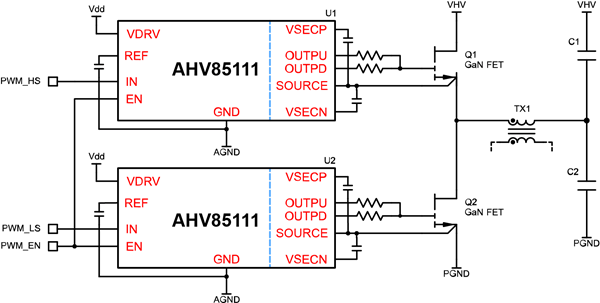
Figure 1: Typical AHV85111 half-bridge application—eliminates high-side bootstrap
| Part Number | Switch | #Channels | Output | Qualifications | Package | Tape & Reel Detail |
|---|---|---|---|---|---|---|
| Part NumberAHV85111KNHTR | SwitchE-Mode GaN | #Channels1 | OutputBipolar | QualificationsAEC-Q100 Grade 2 |
Package10 mm × 7.66 mm × 2.41 mm 12-pin low-profile surface mount | Tape & Reel Detail13-inch 1500 pieces |
| Part NumberAHV85111KNHLU | Part NumberE-Mode GaN | #Channels1 | OutputBipolar | Qualifications | Package10 mm × 7.66 mm × 2.41 mm 12-pin low-profile surface mount | Tape & Reel Detail13-inch 200 pieces |
| Characteristics | Symbol | Notes | Rating | Unit |
|---|---|---|---|---|
| CharacteristicsDrive Supply Voltage | SymbolVDRY | NotesVDRV, wrt to GND | RatingVGND – 0.5 to 15 | UnitV |
| CharacteristicsInput Data | SymbolVIN | NotesIN, wrt to GND | RatingVGND – 0.5 to 15 | UnitV |
| CharacteristicsEnable | SymbolVEN | NotesEN, wrt to GND |
RatingVGND – 0.5 to 15 | UnitV |
| CharacteristicsSelect | SymbolVSEL | NotesSEL to GND; internal use only | RatingVGND – 0.5 to 15 | UnitV |
| CharacteristicsReference Voltage | SymbolVREF | Notes3.3 V reference, wrt GND | RatingVGND – 0.5 to 4 | UnitV |
| CharacteristicsFeedback Voltage | SymbolVFB | Notes1.225 V feedback, wrt SOURCE | RatingVSECN – 0.5 to 15 | UnitV |
| CharacteristicsOutput Drive Pull-Up | SymbolVOUTPU | NotesOUTPU to SOURCE | RatingVSECN – 0.5 to 15 | UnitV |
| CharacteristicsOutput Drive Pull-Down | SymbolVOUTPD | NotesOUTPD to SOURCE | RatingVSECN – 0.5 to 15 | UnitV |
| CharacteristicsIsolated Bias Supply | SymbolVSECP – VSECN | NotesTotal rail | Rating–0.5 to 15 | UnitV |
| CharacteristicsJunction Temperature | SymbolTJ | Notes | Rating–40 to 150 | Unit°C |
| CharacteristicsStorage Temperature | SymbolTSTG | Notes | Rating–40 to 150 | Unit°C |
[1] Stresses beyond those listed under Absolute Maximum Ratings may cause permanent damage to the device. These are stress ratings only, and functional operation of the device at these or any other conditions beyond those indicated in the operational sections of the specifications is not implied. Exposure to absolute maximum rating conditions for extended periods may affect device reliability.
| Characteristic | Symbol | Test Conditions | Value | Unit |
|---|---|---|---|---|
| CharacteristicHuman Body Model | SymbolVHBM | Test Conditions |
Value±2 | UnitkV |
| CharacteristicCharged Device Model | SymbolVCDM | Test Conditions | Value±500 | UnitV |
| Characteristic | Symbol | Test Conditions [1] | Value | Unit |
|---|---|---|---|---|
| CharacteristicJunction-to-Ambient Thermal Resistance | SymbolRθJA | Test Conditions [1]4-layer PCB based on JEDEC standard, with no thermal vias | Value102 | Unit°C/W |
[1] Additional thermal information available on the Allegro website
Valid at –40°C < TJ < 125°C, 10.8 V < VDRV < 13.2 V, CSEC(NET) = 47 nF, COUT = 1 nF, unless otherwise stated. [1][2]
| Characteristics | Symbol | Test Conditions | Min. | Typ. [3] | Max. | Unit |
|---|---|---|---|---|---|---|
| SUPPLY VOLTAGE PINS | ||||||
| Drive Supply Voltage | VDRV | 10.8 | – | 13.2 | V | |
| INPUT PINS | ||||||
| Input Data | VIN | VGND | – | VDRV | V | |
| Enable Active High | VEN | VGND | – | VDRV | V | |
| Select | VSEL | Internal use only | VGND | – | VDRV | V |
| OUTPUT PINS | ||||||
| Isolated Supply Referenced to SOURCE | VSECP | – | – | 6 | V | |
| VSECN | –6 | – | – | V | ||
| VSEC Pin Capacitor CSEC [3] | CSECP | External capacitance connected between VSECP and SOURCE pins; external COUT = 1 nF | 22 [4] | 100 | 300 [5] | nF |
| CSECN | External capacitance connected between VSECN and SOURCE pins; external COUT = 1 nF | 22 [4] | 100 | 300 [5] | nF | |
| CSECPN | External capacitance connected between VSECP and VSECN pins; external COUT = 1 nF | 22 [4] | 100 | 300 [5] | nF | |
| Reference | VREF | 3V3 rail decoupling capacitor pin | VGND | – | 3.3 | V |
| REF Pin Capacitor CREF | CREF | External capacitor connected between REF and GND pin | 100 | – | 1000 | nF |
| Junction Temperature | TJ | –40 | – | 125 | °C | |
[1] CSEC(NET) is the net equivalent of CSECP in series with CSECN, i.e., (CSECP × CSECN) / (CSECP + CSECN).
[2] Not tested in production; guaranteed by design and bench characterization.
[3] Typical values should be chosen to match the ratio of VSECP to VSECN.
[4] Smaller CSEC values than the recommended typical value can give higher voltage ripple on CSEC.
[5] Larger CSEC values will mean longer startup times.
| Characteristic | Symbol | Test Conditions | Value | Unit | ||
|---|---|---|---|---|---|---|
| General | ||||||
| External Clearance | CLR | Shortest terminal-to-terminal distance through air | 8.4 | mm | ||
| External Creepage | CPG | Shortest terminal-to-terminal distance across the package surface | 8.4 | mm | ||
| Distance Through Insulation | DTI | Internal insulation thickness | 200 | µm | ||
| Comparative Tracking Index | CTI | According to IEC 60112 | 400 to 599 | V | ||
| Material Group | MG | According to IEC 60664-1 | II | – | ||
| Overvoltage Category | Per IEC 60664-1 at 600 V line voltage | I–IV | – | |||
| Maximum Reinforced Working Voltage [1][2] | VIORM | Maximum approved working voltage for basic insulation according to UL 62368-1:2014 (Edition 2) | 1000 | VPK VDC | ||
| 700 | VRMS | |||||
| Maximum Impulse Voltage | VIMP | Tested to UL 62368 Table D1 circuit 3 | 8000 | VPK | ||
| Maximum Transient Isolation Voltage | VIOTM | 60 second rating, 100% production test, 1 second at 6000 VRMS | 7000 | VPK | ||
| Maximum Surge Isolation Voltage | VIOSM | Tested with to UL 62368 Table D1 circuit 3 in oil at 1.6 × rating | 8000 | VPK | ||
| Partial Discharge | qPD | Method B1: At routine test (100% production) and preconditioning (type test), Vini = VIOTM, tini = 1 s; Vm = 1.875 × VIORM, tm = 1 s | ≤5 | pC | ||
| Barrier Capacitance, Input to Output | CIO | VIO = 0.5 × sin (2πft), f = 1 MHz | <1 | pF | ||
| Insulation Resistance, Input to Output | RIO | >1012 | Ω | |||
| Climatic Classification | 40/105/21 | – | ||||
| UL1577 | ||||||
| Withstand Isolation Voltage | VISO | 60 second rating, 100% production test, 1 second at 6000 VRMS | 5000 | VRMS | ||
[1] Pending certification to UL 62368 Edition 2.
[2] Working Voltage evaluated for use at Pollution Degree 2 and Material Group II.
| Device | MSL Rating | Maximum Floor Life at Standard Ambient (30°C/60%RH) | Maximum Peak Reflow Temperature | Pre-Reflow Bake Requirement |
|---|---|---|---|---|
| DeviceAHV85111 | MSL RatingMSL-3 | Maximum Floor Life at Standard Ambient (30°C/60%RH)168 hours | Maximum Peak Reflow Temperature260°C | Pre-Reflow Bake RequirementPer JEDEC J-STD-033C |
Per JEDEC J-STD-033C, the AHV85111 devices are rated MSL3. This MSL3 rating means that once the sealed production packaging is opened, the devices must be reflowed within a “floor-life” of 168 hours (1 week) if they are stored in under standard ambient conditions (30°C and 60% relative humidity (RH)).
The peak reflow temperature should not exceed the maximum specified in MSL Rating table.
If the devices are exposed to the standard ambient for more than 168 hours, they must be baked before reflow to remove any excess moisture in the package and prevent damage during reflow soldering. The required bake times and temperatures are detailed in IPC/JEDEC standard J-STD-033C. If the devices are exposed to higher temperature and/or RH compared to the standard ambient of 30°C/60% RH, the floor-life will be shortened due to the increased rate of moisture absorption. If the actual ambient conditions exceed the standard ambient, it is recommended that parts should always be baked per IEC/JEDEC J-STD-033C before reflow as a precaution to avoid potential device damage during reflow soldering.
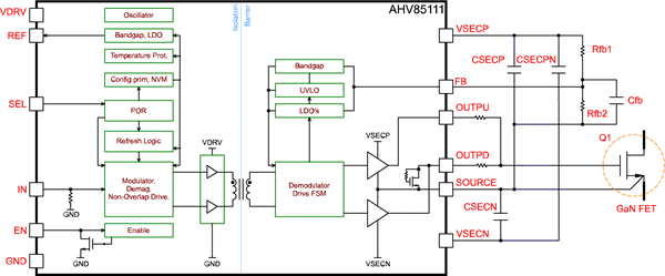
Figure 2: AHV85111 Block Diagram
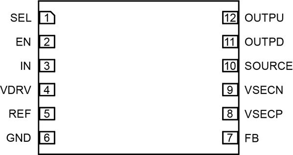
Package NH Pinout (Top View)
| Number | Name | Function |
|---|---|---|
| Number1 | NameSEL | FunctionInternal use only—this pin must be tied high to VDRV. |
| Number2 | NameEN | FunctionBidirectional enable pin; see Figure 3. |
| Number3 | NameIN | FunctionPWM input; see Electrical Characteristics table. |
| Number4 | NameVDRV | FunctionGround referenced voltage supply; this voltage indirectly sets the total output-side bias rail amplitude. |
| Number5 | NameREF | FunctionConnection for external decoupling capacitor for internal REF rail; can be used to power external low current loads up to 2 mA. |
| Number6 | NameGND | FunctionGround pin for input/primary side. |
| Number7 | NameFB | FunctionFeedback pin to adjust the regulated VSECP level. |
| Number8 | NameVSECP | FunctionPositive regulated isolated gate drive bias rail; external decoupling capacitor referenced to SOURCE. |
| Number9 | NameVSECN | FunctionNegative unregulated isolated gate drive bias rail; external decoupling capacitor referenced to SOURCE. |
| Number10 | NameSOURCE | FunctionIsolated output return pin. |
| Number11 | NameOUTPD | FunctionIsolated output drive pull-down pin; see Electrical Characteristics table. |
| Number12 | NameOUTPU | FunctionIsolated output drive pull-up pin; see Electrical Characteristics table. |
| Characteristics | Symbol | Test Conditions | Min. | Typ. | Max. | Unit |
|---|---|---|---|---|---|---|
| SUPPLY CURRENTS | ||||||
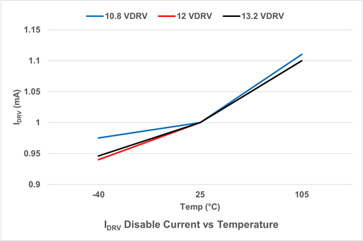
| CharacteristicsVDRV Disable Current | SymbolIDRV_DIS | Test ConditionsVIN = 0, EN = 0 | Min.– | Typ.1 | Max.1.3 | UnitmA |
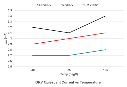
| CharacteristicsVDRV Quiescent Current | SymbolIDRV_Q | Test ConditionsVIN = 0, EN = 1 | Min.– | Typ.2 | Max.3.4 | UnitmA |
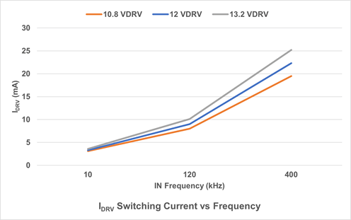
| CharacteristicsVDRV Switching Current | SymbolIDRV_SW | Test ConditionsfS = 120 kHz, EN = 1 | Min.– | Typ.9.5 | Max.13 | UnitmA |
| INPUT PINS | ||||||
| CharacteristicsInput Data – Logic Low | SymbolVIN(L) | Test Conditions | Min.– | Typ.– | Max.0.8 | UnitV |
| CharacteristicsInput Data – Logic High | SymbolVIN(H) | Test Conditions | Min.2.0 | Typ.– | Max.– | UnitV |
| CharacteristicsInput Data Hysteresis | SymbolVIN(HYS) | Test Conditions | Min.– | Typ.300 | Max.– | UnitmV |
| CharacteristicsEnable Active High – Logic Low | SymbolVEN(L) | Test Conditions | Min.– | Typ.– | Max.0.8 | UnitV |
| CharacteristicsEnable Active High – Logic High | SymbolVEN(H) | Test Conditions | Min.2.0 | Typ.– | Max.– | UnitV |
| CharacteristicsEnable Active High – Hysteresis | SymbolVEN(HYS) | Test Conditions | Min.– | Typ.400 | Max.– | UnitmV |
| CharacteristicsInternal On-Chip Pull-Down Resistance On IN Pin | SymbolRIN | Test ConditionsTA = 25°C | Min.– | Typ.300 | Max.– | UnitkΩ |
| CharacteristicsFB Pin Voltage [2] | SymbolVFB | Test ConditionsFB pin reference wrt VSECP | Min.1.1 | Typ.1.225 | Max.1.35 | UnitV |
| OUTPUT PINS | ||||||
| CharacteristicsOUTPU Pull-Up Resistance | SymbolRPU | Test Conditions | Min.1.5 | Typ.2.8 | Max.3.5 | UnitΩ |
| CharacteristicsOUTPD Pull-Down Resistance | SymbolRPD | Test Conditions | Min.0.5 | Typ.1.0 | Max.1.7 | UnitΩ |
| CharacteristicsReference Voltage | SymbolVREF | Test ConditionsRegulation level | Min.– | Typ.3.30 | Max.– | UnitV |
| CharacteristicsReference Current | SymbolIREF | Test ConditionsAvailable source current | Min.– | Typ.2 | Max.– | UnitmA |
| CharacteristicsHigh Level Source Current [2] | SymbolISOURCE | Test ConditionsVSEC = 5.4 V, Rext_pu = 0 Ω, COUT = 10 nF | Min.– | Typ.2 | Max.– | UnitA |
| CharacteristicsLow Level Sink Current [2] | SymbolISINK | Test ConditionsVSEC = 5.4 V, Rext_pd = 0 Ω, COUT = 10 nF | Min.– | Typ.4 | Max.– | UnitA |
| PRIMARY UNDERVOLTAGE LOCKOUT | ||||||
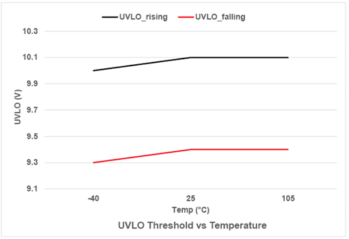
| CharacteristicsVDRV UV Threshold, Rising [3] | SymbolVDRV_UVH | Test Conditions | Min.9.5 | Typ.10.0 | Max.10.5 | UnitV |
| CharacteristicsVDRV UV Threshold, Falling [3] | SymbolVDRV_UVL | Test Conditions | Min.8.8 | Typ.9.3 | Max.9.8 | UnitV |
| CharacteristicsVDRV UV Hysteresis | SymbolVDRV_UVHYS | Test Conditions | Min.0.5 | Typ.0.7 | Max.0.9 | UnitV |
| SECONDARY UNDERVOLTAGE LOCKOUT | ||||||
| CharacteristicsVSEC UV Threshold, Rising | SymbolVSEC_UVH | Test Conditions | Min.4 | Typ.4.4 | Max.4.9 | UnitV |
| CharacteristicsVSEC UV Threshold, Falling | SymbolVSEC_UVL | Test Conditions | Min.3.7 | Typ.4.1 | Max.4.5 | UnitV |
| CharacteristicsVSEC UV Hysteresis | SymbolVSEC_UVHYS | Test Conditions | Min.0.2 | Typ.0.3 | Max.0.4 | UnitV |
| OVERTEMPERATURE PROTECTION | ||||||
| CharacteristicsOvertemperature Threshold, Rising | SymbolTSD | Test Conditions | Min.150 | Typ.155 | Max.160 | Unit°C |
| CharacteristicsOvertemperature Hysteresis | SymbolTSD(HYS) | Test Conditions | Min.– | Typ.30 | Max.– | Unit°C |
[1] Not cold tested in production (–40°C); guaranteed by design and bench characterization.
[2] Not tested in production; guaranteed by design and bench characterization.
[3] When VDRV is below the UVLO threshold, the driver output is actively held low.
Valid at –40°C < TJ < 125°C, 10.8 V < VDRV < 13.2 V, CSEC(NET) = 47 nF, COUT = 1 nF, unless otherwise stated [1]
| Characteristics | Symbol | Test Conditions | Min. | Typ. | Max. | Unit |
|---|---|---|---|---|---|---|
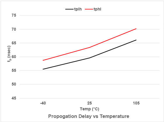
| Characteristics Propagation Delay, High To Low | Symbol tPHL | Test Conditions Rext_pu = 2 Ω | Min. – | Typ. 50 | Max. 100 | Unit ns |
| Characteristics Propagation Delay, Low To High | Symbol tPLH | Test Conditions Rext_pd = 2 Ω | Min. – | Typ. 50 | Max. 100 | Unit ns |
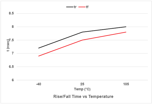
| Characteristics Rise Time | Symbol tr | Test Conditions Rext_pu = 0 Ω, 20-80% | Min. – | Typ. 9 | Max. 15 | Unit ns |
| Characteristics Fall Time | Symbol tf | Test Conditions Rext_pd = 0 Ω, 20-80% | Min. – | Typ. 7 | Max. 15 | Unit ns |
| Characteristics Shortest ON Time Allowable [2] | Symbol tpw(on) | Test Conditions The ON time should never be less than specified minimum | Min. 100 | Typ. – | Max. – | Unit ns |
| Characteristics Shortest OFF Time Allowable [2] | Symbol tpw(off) | Test Conditions The OFF time should never be less than specified minimum | Min. 100 | Typ. – | Max. – | Unit ns |
| Characteristics Wait Time Before First IN Edge is Delivered After VDRV is Within Specification | Symbol tSTART | Test Conditions – | Min. – | Typ. – | Max. 250 | Unit µs |
[1] Not cold tested in production (–40°C); guaranteed by design and bench characterization.
[2] Not tested in production; guaranteed by design and bench characterization.
The AHV85111 is a self-powered isolated gate driver. Allegro’s patented Power-Thru technology allows the transfer of both PWM signal and gate power across a single transformer-based isolation barrier. This eliminates the need to provide an isolated bias supply to power the isolated side of the driver, greatly simplifying the sys- tem design. Only decoupling capacitors and programming resistors are required on the isolated side to generate the bipolar positive and negative gate drive rails VSECP and VSECN.
The AHV85111 driver has been optimized for driving the gate of typical Schottky-gate Enhancement-mode (E-mode) GaN FETs, such as those available from GaN Systems, Innoscience, ST, Nex- peria, GaN Power International, Taiwan Semiconductor, Rohm and others. An online FET selection tool can be downloaded from the Allegro website to assist system designers, to check compat- ibility of various FET devices with the driver.
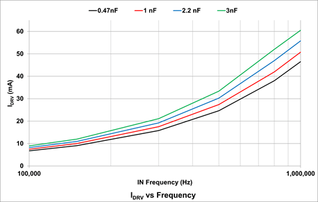
The isolated VSECP positive bias rail is locally regulated, using an external resistor divider connect to the FB pin. The balance of the secondary bias voltage becomes the unregulated negative rail VSECN. The VSECP rail regulates quite well versus PWM switching frequency fSW at the IN pin, for a given fixed VDRV level, and for a fixed load COUT at the OUTx drive pins—the load presented by the gate of the GaN FET being driven as long as the QG(TOT) versus frequency recommended operating area (ROA) curve recommendations are adhered to; see Figure 10 ROA curve. This is because the charge delivered per PWM cycle naturally increases in tandem with the charge consumed by the FET gate, so there is a good charge balance across a wide frequency range.
However, the VSEC rails do vary with effective loading of the gate of FET being driven; as VSEC levels fall, more charge is available to be delivered to the secondary side, while the charge consumed by the FET gate decreases with falling VSEC levels. Therefore, the VSEC rails will droop as far as needed until the charge delivered matches the charge consumed. For this reason, it is also very important to minimize the amount of charge diverted into any external loads. For example, a very low bias power external circuit can be powered using VSEC, but the consumption should be minimal, to minimize the charge diverted away from the gate of FET. Similarly, if a gate-source pull-down resistor is desired on the load FET (to prevent false turn-on in the case of a manufacturing fault, such as an open-circuit gate turn-on resistor), the resistor value should be as large as possible. The recommended value is 100 kΩ, to minimize DC loading on VSEC. Since DC load current converts to equivalent charge as Q = I × t, DC loading effects will become significantly more pronounced at lower PWM frequency, as the time duration t gets longer. In particular, it should be noted that the driver will attempt to regulate the positive rail VSECP as priority, with the balance of charge diverted to create the negative rail VSECN. In certain situations, such as low VDRV, high load FET QG, excessive external loading of VSEC, high load FET gate leakage current IGSS, or a combination of these, there may be be insufficient charge available to create a sufficient or even any negative VSECN. However, the ROA curve in Figure 10 indicates the supported operating range of QG versus PWM frequency that maintains a minimum VSECN negative rail of –1 V or better.
Since there is just a single magnetic isolation barrier to transfer both PWM signal and gate power, this also greatly reduces the total parasitic capacitance between the primary-side and isolated side, to typically < 1 pF total for both signal and power channels. This is much less than the typical total parasitic capacitance value for a solution using a conventional isolated gate driver with a separate isolated DC-DC bias supply, where the capacitance contribution from the DC-DC isolation transformer could be as high as 10 pF or more. This reduction in isolation capacitance greatly reduces the level of noise injected back into the low-voltage control circuit by the high-voltage and high dv/dt switching nodes in the power stage half-bridge legs, reduces system level CommonMode (CM) EMI, and saves on power loss that occurs through repetitive charging and discharging of this parasitic capacitance between the high bus voltage level and ground.
EN is a bidirectional open-drain pin which requires an external resistor pull-up to the VDRV pin. The EN pin allows for management of startup and fault conditions between the PWM controller and multiple drivers, through use of a shared enable EN line. Either the PWM controller or the driver can pull the EN pin low via the EN bus, as shown in Figure 3. When the EN pin is pulled low (either externally or internally), this forces the driver into a mode where the IN pin signal is ignored, and the OUT pins are disabled and actively pulled low. When the EN pin goes high, normal driver operation is enabled.
In the event of an internal driver fault condition, such as UVLO or normal startup delay, the EN pin is actively pulled low internally by the driver. This driver pull-down can be detected by the PWM controller and used as a flag for an external fault, or to flag that the driver is ready, and PWM can commence.
The shared EN line is typically wired-AND with the controller EN pin, as shown in Figure 3. Multiple drivers can be connected in parallel with the controller on the shared EN line, such that all connected drivers will hold the EN line low until all drivers and the PWM controller have released their own EN pin, ensuring smooth safe startup of the system.
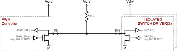
Figure 3: Example Wired-AND connection between driver and controller
Note that the EN pin has no internal pull-up or pull-down—the open-drain configuration relies on an external pull-up resistor for normal operation. Similarly, the EN pin must be actively pulled low externally to disable the driver. The EN pin should never be left floating or connected directly to VDRV or any other system bias voltage; a pull-up resistor must be used. The EN pin should be connected to VDRV through a pull-up resistor in a recommended range of 10 to 100 kΩ. The EN pin dv/dt when being pulled low or high should be at least 0.1 V/μs.
When the EN pin is pulled low, the driver output is disabled, and pulls down the OUTPD pin, regardless of the IN pin level (high or low). The driver goes to a low-power standby mode, and the isolated VSECP and VSEPN bias rails are allowed to discharge. The rate of decay of VSECP and VSECN depends on the value of the CSECP and CSECN capacitors.
When the EN pin is subsequently pulled high, the driver will re-enable, and the isolated VSEC bias rail will start to recharge. Even if the IN pin is connected to a PWM signal, the OUT pins will not respond until the VSECP rail exceeds the secondary UVLO threshold. The rate of rise of VSECP depends on the PWM frequency at the IN pin. Worst-case slowest rise time is when IN = 0, using the slowest internal energy transfer mode. In this mode, the rise time will be approximately 250 μs for equivalent CSEC of 47 nF to charge from zero to the rising UVLO threshold.
Any PWM signal applied to IN must remain low until VDRV > UV threshold, to avoid parasitic charging of the VDRV rail through the IN pin internal ESD structures. After VDRV exceeds the UV rising threshold, a startup time delay tSTART is required to allow all internal circuits to initialize and stabilize. During tSTART, any IN signal inputs are ignored. EN internal pull-down will remain active during tSTART, and will release (i.e., go open-drain) only when VDRV has reached its UVLO voltage level, all on-chip voltages are stabilized, there is no overtemperature fault, and the internal tSTART timer has elapsed. Thus, the EN pin can be used via a shared EN line to flag when tSTART has elapsed, and the driver is ready to respond to PWM signals at the IN pin, as outlined above.
Typical startup waveforms are shown in Figure 4.
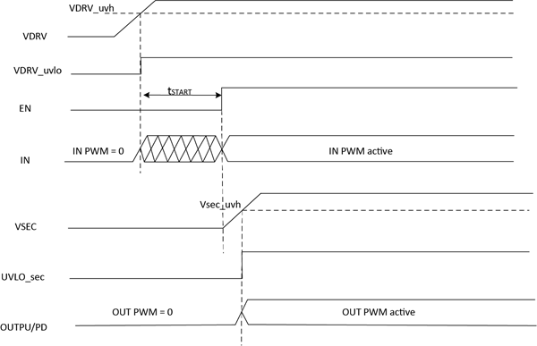
Figure 4: AHV85111 Startup Mechanism
Once VDRV drops below UVLO falling threshold, the enable signal is pulled down and the driver output shuts down. The rate of decay of VSEC is determined by the VSEC capacitance as shown in Figure 5.
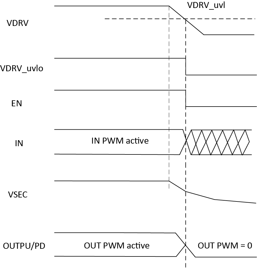
Figure 5: Shutdown Mechanism
In cases when IN-PWM signal frequency is low or when IN is set to continuous 1 or 0, in order to prevent VSEC voltage decay, the AHV85111 implements an internal clock of 12 µs (tREFRESH). When tREFRESH elapses, the driver recharges VSEC rail to maintain output voltage. This condition persists until IN changes state as shown in Figure 6.
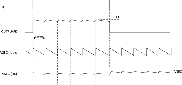
Figure 6: AHV85111 Refresh Mechanism
As shown in Figure 7, the feedback (FB) pin is used in conjunction with two resistors RFB1 and RFB2 to set the regulated output voltage between VSECP and SOURCE pins.
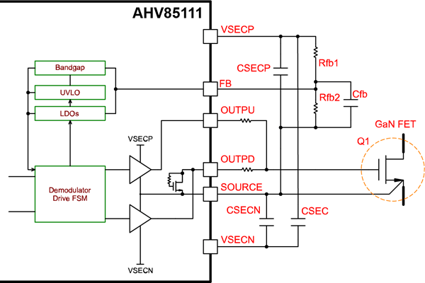
Figure 7: Rfb1 and Rfb2 used to set the desired
VSECP-to-SOURCE positive bias rail regulation level
Decoupling capacitors CSECP and CSECN are connected from VSECP to SOURCE and VSECN to SOURCE respectively, to supply the peak gate charge and discharge currents. In addition, a capacitor CSECPN should be connected directly from VSECP to VSECN to ensure stability of the internal LDO—a value of 100 nF is recommended. A small noise filter cap is also recommended to be placed from FB to SOURCE to improve VSECP regulation robustness to noise. Typically 100 pF is recommended for RFB2 = 100 kΩ
Table 1 shows resistance values (nearest E96 standard value) and associated outputs for an input voltage of VDRV = 12 V, for typical VSECP target setpoints. For other required VSECP levels, Equation 1 can be used to calculate the required value for RFB1, assuming that the VDRV level is high enough to allow VSECP to regulate.
Table 1: VSECP – VSOURCE vs. Rfb1 value; Rfb2 = 100 kΩ, VDRV = 12 V
| VSECP – VSOURCE (V) | Rfb1 (kΩ) |
|---|---|
| 5.0 | 32.4 |
| 5.4 | 29.4 |
| 6.0 | 25.5 |
The positive output voltage is regulated on-chip with respect to the SOURCE pin, at the level set by choice of RFB2, assuming that the VDRV level is sufficient to allow regulation at the target VSECP level. The remaining voltage overhead, unregulated, is the negative voltage drive (stored on CSECN).
Figure 8 shows curves of the typical positive output voltage range as a function of the input voltage VDRV. Note that if the VDRV level is too low to allow VSECP to achieve regulation, VSECN will be clamped to zero. Once the VDRV level is sufficient to allow VSECP to regulate, and excess secondary bias voltage will then appear on the negative rail VSECN
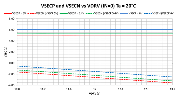
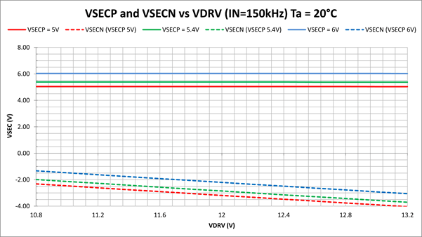
Figure 8: Positive and negative output voltage vs. input VDRV
At high operating ambient temperatures and low input PWM frequencies below 100 kHz, the total secondary-side bias rail, VSECP – VSECN, is reduced. Figure 9a shows that for minimum input supply voltage, VDRV, and maximum recommended 6 V output set point, VSECP, the total secondary-side bias voltage is not sufficient to maintain regulation of VSECP and VSECN is subsequently zero volts. Increasing VDRV provides more secondary bias voltage and regulation is achieved.
At higher input frequencies, above 100 kHz, there is no reduction in VSECP – VSECN at maximum ambient temperature. Figure 9b shows there is sufficient secondary-side bias voltage to maintain regulation across the full input voltage range.
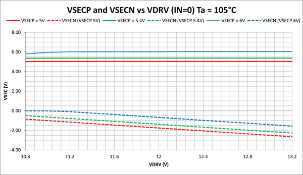
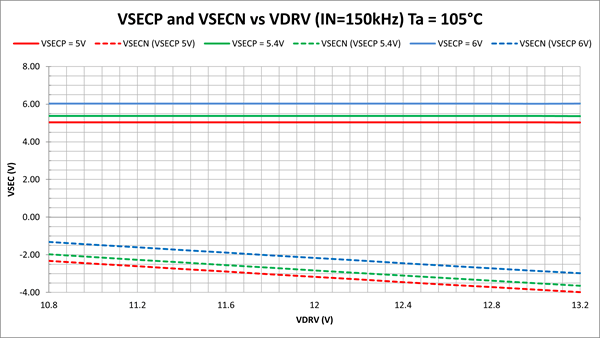
Figure 9: Effect of high ambient temperature
on VSECP and VSECN
The maximum recommended PWM frequency is 1 MHz. However, the device internal dissipation, application PCB layout, and ambient temperature must also be taken into account to ensure that the internal recommended TJ(MAX) of 125°C is not exceeded.
Figure 10 shows the recommended operating area curve of QG(TOT) versus PWM frequency that will maintain a negative rail VSECN of at least –1 V at nominal VDRV of 12 V. Operating further below this curve will result in even more negative off-state volt- age VSECN. The AHV85111 can be operated above the curve of Figure 10, but the negative rail VSECN will be limited, and in some cases can be close to zero.
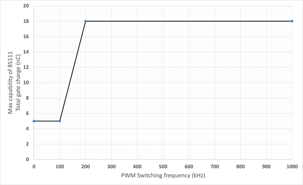
Figure 10: Recommended Operating Area Curve Max QG(TOT) as a function of PWM Frequency fSW, VDRV = 12 V
The thermal derating curves of Figure 11 are based on the device thermal performance using JEDEC-standard PCB footprint and PCB design (layer count and size of copper planes for heatsinking). The actual thermal performance in the end system design should always be verified, since every system is different in terms of exact PCB design and ambient airflow from natural or forced convection
Because of the required creepage distance under the IC package to meet system safety requirements, it is not allowed to put a large copper plane under the IC for heatsinking purposes. Instead, it is recommended that the primary-side GND pins and secondary-side SOURCE pins be connected to appropriate ground planes on each side, and to maximize the size of these planes to maximize thermal performance. Multiple thermal vias to larger inner-layer ground planes can also help improve thermal performance.
The effective gate capacitance COUT that loads the OUTx drive pins can be estimated from the GaN FET datasheet. The FET total charge QG(TOT) is usually specified in nC, for a given VGS voltage swing.
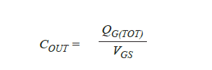
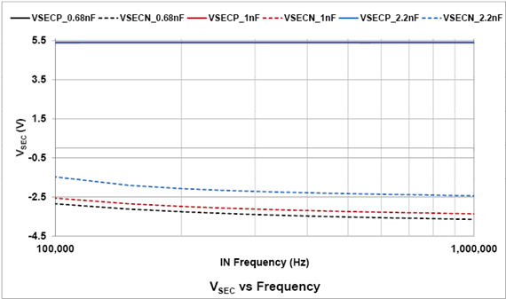
Knowing the value of COUT, the expected level of the second- ary supply rail VSEC can be estimated from VSEC vs. Frequency from Typical IC Characteristics curve. From COUT, VSEC and the required PWM frequency FSW, the total gate power can be calculated as follows:
Note that VSEC in this case is the full VGS voltage swing from posirtive to negative, i.e., VGS = VSECP – VSECN. In practice, the system design will likely use external gate resistors to con- trol the FET turn-on and turn-off speed. The gate-drive power consumption PGATE will be dissipated by the internal driver FET resistances and the external resistors, apportioned by the ratio of the resistances. The larger the value of the external resistors, the higher the power dissipation in those resistors, and the lower the dissipation in the internal driver resistances. To simplify the thermal estimates, and to add in design margin, it is assumed that all of the PGATE power is dissipated inside the driver package.
The internal driver stage MOSFETs will consume drive power, and they will have switching losses, so there is an efficiency factor that needs to be accounted for when estimating the internal power consumed when delivering the PGATE power.
Finally, the internal isolated bias power stage consumes power. As well as the IC quiescent power consumption, there are also drive, conduction and switching losses in the internal power FETs that drive and rectify the energy transfer through the internal isolation transformer, as well as the conduction and core losses of the transformer. These losses scale approximately linearly with PWM frequency.
Combining all of these loss mechanisms, the total package power dissipation (in mW) can be estimated using the following empirical formula, where fSW is in kHz and PGATE is in mW. This assumes a fixed VDRV level of 12 V.
Using the standard JEDEC thermal impedances in the thermal characteristics table, the maximum allowed ambient temperature TA can be estimated from:
Alternatively, Figure 11 can be used to graphically estimate the allowable TA(MAX) as a function of FSW and COUT. The online FET selection tool can also be used to estimate expected driver temperature rise over ambient, and maximum allowed TA.
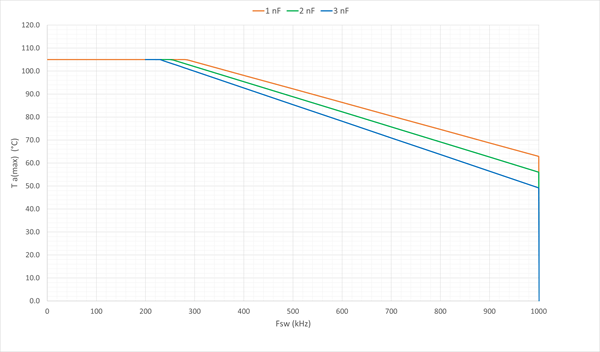
Figure 11: AHV85111 thermal derating curve as a function of load capacitance COUT and PWM frequency fSW
What follows is an example calculation, based on the APE-K85110KNH-01-T-MH evaluation board. Assume the target switching frequency is 400 kHz, and the required maximum ambient temperature is 85°C.
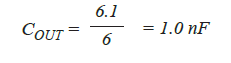
The FET used on the board is a GS-66516-B from GaN Systems. From the GaN datasheet, the QG(TOT) is specified at 14.2 nC at 6 V VGS swing. Therefore, the equivalent COUT is:
From figure 8, for this value of COUT the VSEC level can be estimated as approximately 7.5 V. Note that this evaluation board uses an external Zener circuit to limit the positive VGS swing to approximately 6.2 V, with the balance of the VSEC voltage appearing as a negative VGS in the off-state. Nevertheless, the full VGS swing must be used to estimate the gate power dissipation.

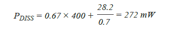
From this, the total package power dissipation can be estimated:
Now the maximum allowed ambient temperature can be verified to ensure that it meets the system requirement:
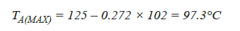
This equation shows that the design can meet the required maximum ambient temperature. However, as noted above, this uses RTH(JA) estimates based on standardised JEDEC footprints and PCB layouts; the actual thermal performance must be verified in each individual application.
The maximum allowed ambient temperature can also be readily estimated from the curves in figure 7. Using FSW of 400 kHz, and COUT of approximately 2.4 nF, the estimate TA(MAX) is approximately 96°C, which is close the calculated result using the empirical loss estimation.
The output gate drive amplitude is always less than VDRV due to internal impedances and voltage drops.
The total secondary-side bias rail, VSECP – VSECN, depends on the VDRV level applied on the primary, and effective CLOAD presented by the GaN FET being driven. CLOAD = QG(TOT) / VGATE, i.e., the total gate charge at a specified VGATE, divided by VGATE. CISS is not an equivalent measure of CLOAD. CISS is a small signal equivalent capacitance, whereas CLOAD is a large-signal equivalent.
The recommended value for CSEC(NET) is approximately 10 to 20 times CLOAD (the equivalent gate capacitance), to give approximately 5% to 10% switching ripple on the VSEC rails. Other values are possible; however, lower values will result in higher ripple. Larger CSEC(NET) value will require a longer startup time. The maximum recommended value of CSEC(NET) = 100 nF should not be exceeded.
Figure 12 shows a typical application for driving a GaN transistor with a bipolar drive arrangement.
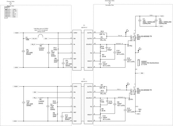
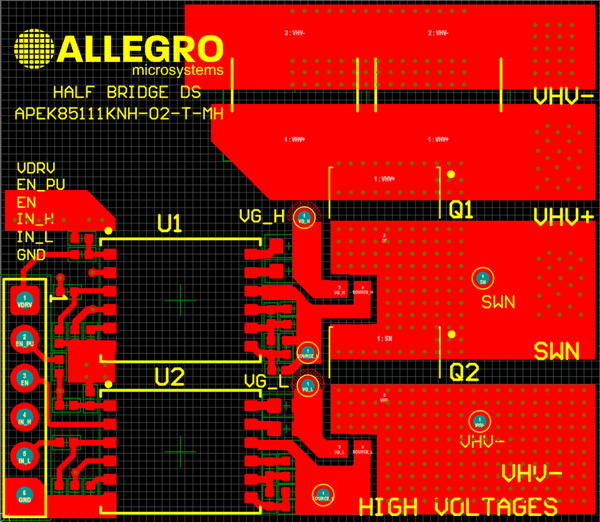
Figure 12: APEK85111KNH-02-T-MH schematic for driving a GaN transistor with a bipolar drive arrangement
APEK85111KNH-02-T-MH is a design example for half bridge gate driver with GaN transistors. There is also a bipolar output drive
configuration for additional protection against false turn-on events. The design parameters are shown in Table 2.
| Parameter | Value | Unit |
|---|---|---|
| ParameterVDRV | Value10.8–13.2 | UnitV |
| ParameterMaximum Switching Frequency | Value1000 [1] | UnitkHz |
| ParameterCSEC(NET) | Value50 | UnitnF |
| ParameterVSECP Voltage | Value5.4 | UnitV |
| ParameterVSEC_RIPPLE | Value5–10 | Unit% |
[1] Frequency depends on factors like heat sinking, temperature, high voltage decoupling capacitance and IN PWM duty cycle range
The following are some key points to consider while doing the PCB layout for the best performance with AHV85111:
Further detailed PCB layout guidelines are available in the application note Design and Application Guide for the AHV85111.
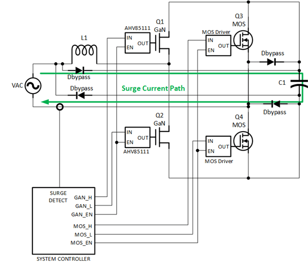
During various system-level events, large transient currents can flow for short periods. Examples of this include lightning surge testing to IEC61000-4-5, and system-level ESD testing to IEC61000-4-2. During these events, the large transient currents that flow can also create large stray magnetic fields, and these can also couple unintentionally to the isolated gate driver.
It is recommended to use the driver enable (EN) pin to achieve a power-train “safe-state” during such external transient events. An example of the use of this safe-state architecture is shown in Figure 14, for a Totem-Pole PFC power stage. When a surge event is detected, the system controller inhibits the PWM gate drive signal to both GaN and MOS legs, and also pulls down the open-drain Enable (EN) lines to all drivers. This puts the power train into a safe state and ensures a robust response to the surge event.
For further details, refer to the application note Design and Application Guide for the AHV85111
You can now download the datasheet by clicking the link below